
Silica glass micro-optics 3D printed on optical fibre tips
Researchers say that this achievement is a first for communications and bridges the gap between 3D printing and photonics, with a wide range of potential applications including sensors and quantum communication
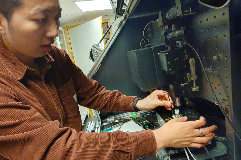
Researchers in Sweden 3D printed silica glass micro-optics on the tips of optical fibres – surfaces as small as the cross section of a human hair. The achievement, which the team says is a first for communications, could enable faster internet and improved connectivity, as well as innovations like smaller sensors and imaging systems.
Reporting in the journal ACS Nano, researchers at KTH Royal Institute of Technology in Stockholm say integrating silica glass optical devices with optical fibres enables multiple innovations, including more powerful remote sensors for environmental and healthcare applications. They add that their printing techniques could also prove valuable in the production of pharmaceuticals and chemicals.
According to KTH Professor Kristinn Gylfason, the method overcomes long-standing limitations in structuring optical fibre tips with silica glass, which often require high-temperature treatments that compromise the integrity of temperature-sensitive fibre coatings.
In contrast to other methods, the process begins with a base material that doesn’t contain carbon, meaning that high temperatures are not needed to drive out carbon in order to make the glass structure transparent. The authors have filed a patent application for the technique.
More resilient sensors
The study’s lead author, Lee-Lun Lai, says the researchers printed a silica glass sensor that proved more resilient than a standard plastic-based sensor after multiple measurements.
“We demonstrated a glass refractive index sensor integrated onto the fibre tip that allowed us to measure the concentration of organic solvents,” said Lai. “This measurement is challenging for polymer-based sensors due to the corrosiveness of the solvents.”
A co-author of the study, Po-Han Huang, added: “These structures are so small you could fit 1000 of them on the surface of a grain of sand, which is about the size of sensors being used today.”
The researchers also demonstrated a technique for printing nanogratings, ultra-small patterns etched onto surfaces at the nanometre scale. These are used to manipulate light in precise ways and have potential applications in quantum communication.
Gylfason says the ability to 3D print arbitrary glass structures directly on fibre tip opens new frontiers in photonics. “By bridging the gap between 3D printing and photonics, the implications of this research are far-reaching, with potential applications in microfluidic devices, MEMS accelerometers and fibre-integrated quantum emitters.”
Image credit: David Callahan


