Cadence and TSMC extend collaboration on semiconductor design

The companies have announced several technology developments, including a silicon photonics design flow to support TSMC’s Compact Universal Photonic Engine (COUPE) 3D photonics process
Cadence Design Systems and TSMC have extended their longstanding collaboration by announcing a range of technology advancements intended to accelerate design, including developments ranging from 3D-IC and advanced process nodes to design IP and photonics. Cadence says that these joint efforts significantly advance system and semiconductor design for AI, automotive, aerospace, hyperscale and mobile applications.
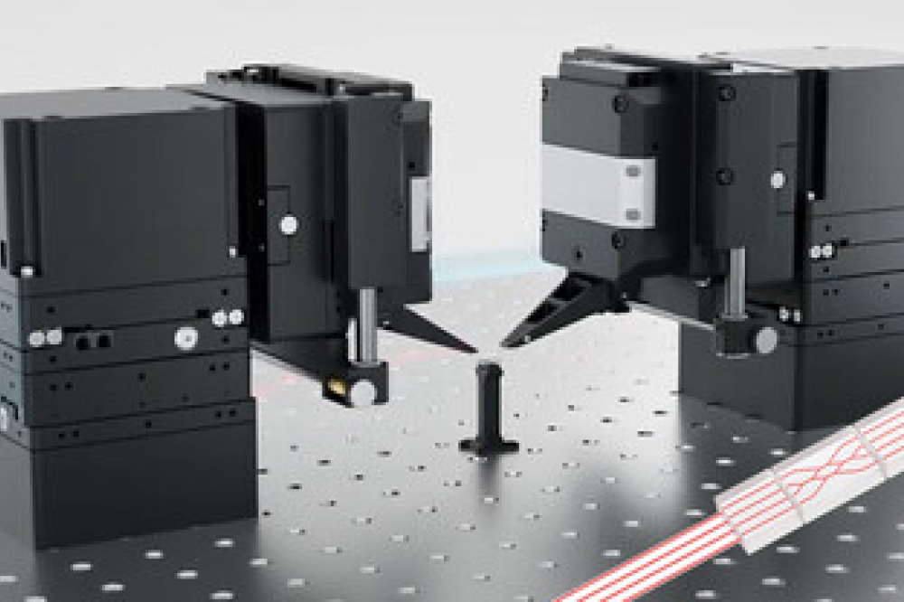
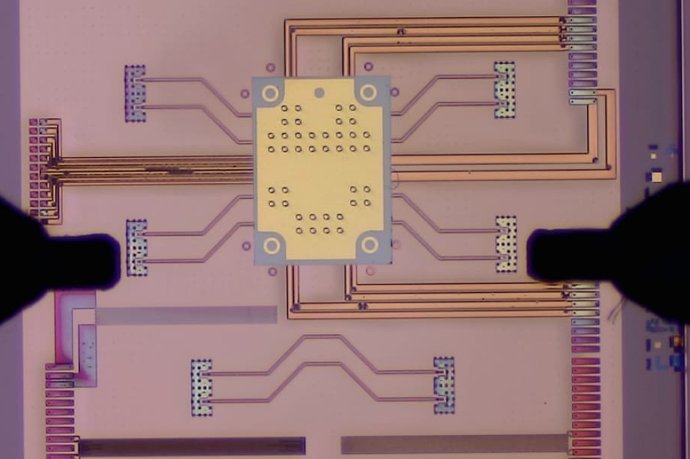
Among the technology achievements to emerge from this partnership is a new silicon photonics flow to support TSMC’s Compact Universal Photonic Engine (COUPE) technology. The companies have collaborated to develop a design flow for the COUPE 3D photonics process that features the Cadence Integrity 3D-IC platform. The TSMC COUPE technology enables the heterogeneous integration of photonic ICs with electrical ICs while minimising coupling losses.
According to Cadence, its developing design flow seeks to support TSMC’s COUPE technology and includes the Cadence Spectre X Simulator, Virtuoso Studio, EMX 3D Planar Solver, and Pegasus Verification System, enabling joint customers to meet the most demanding system requirements and pave the way for high-performance computing applications.
Other developments announced include: new features and functionality added to the Integrity 3D-IC platform to enable chiplet assembly and design; the certification of Cadence’s digital solutions for the TSMC N2 design flow; the Cadence Custom/Analog Design Flow being fully certified for TSMC’s latest N2 Process Design Kit (PDK); and the Cadence EMX 3D Planar Solver receiving certification for TSMC’s N5 process technology. Additionally, the companies have released a Virtuoso Studio N16 to N6 RF migration reference flow, intended to substantially reduce turnaround time; and a comprehensive portfolio of IP cores for TSMC’s N3 process.
“We have a distinguished track record collaborating with TSMC to deliver a broad set of innovations across EDA, packaging and IP to accelerate system and semiconductor design and enable customers to achieve aggressive time-to-market goals,” said Chin-Chi Teng, SVP and GM of R&D at Cadence. “These new certified design flows and standardised solutions allow customers to confidently design for TSMC advanced nodes and usher in improved design efficiency and technological advancements.”
Dan Kochpatcharin, head of the Design Infrastructure Management Division at TSMC, added: “TSMC works closely with Cadence to accelerate customer innovation by providing high-quality design tools certified for use with our most advanced processes. Through our longstanding collaboration, we’re able to deliver greater value for the most advanced SoC designs, benefiting from the significant power and performance boost afforded by our latest technology innovations.”


