New technique for precisely manipulating light with minimal loss

Researchers integrate 2D ferroionic materials with silicon to create low-loss tuneable optical platform with numerous potential applications, including environmental sensing, optical imaging, and neuromorphic computing
A team of researchers at NYU Abu Dhabi’s Photonics Research Lab (PRL) have reported a novel, two-dimensional material capable of manipulating light with exceptional precision and minimal loss. This development addresses the increasing demand for efficient, tuneable optical materials capable of precise light modulation to create greater bandwidth in communication networks and advanced optical systems.
Tuneable optical materials (TOMs) are revolutionising modern optoelectronics, electronic devices that detect, generate, and control light. In integrated photonic circuits, precise control over the optical properties of materials is crucial for unlocking groundbreaking and diverse applications in light manipulation. Two-dimensional materials like Transition Metal Dichalcogenides (TMDs) and graphene exhibit remarkable optical responses to external stimuli. However, achieving distinctive modulation across a short-wave infrared (SWIR) region while maintaining precise phase control at low signal loss within a compact footprint has been a persistent challenge.
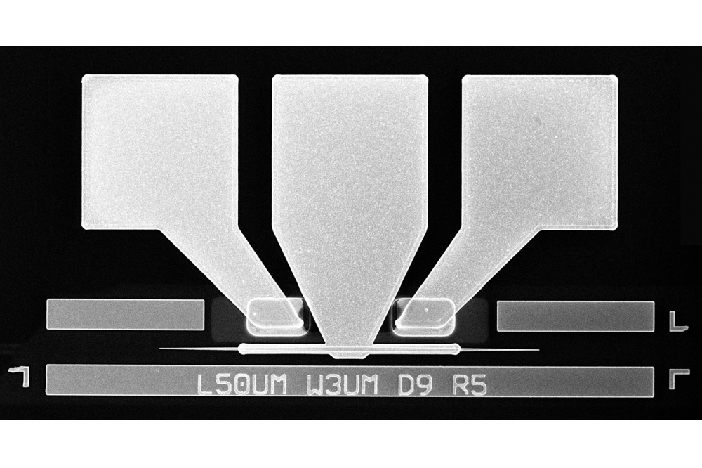
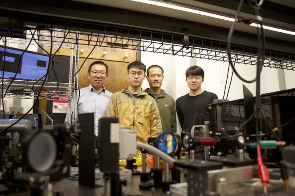
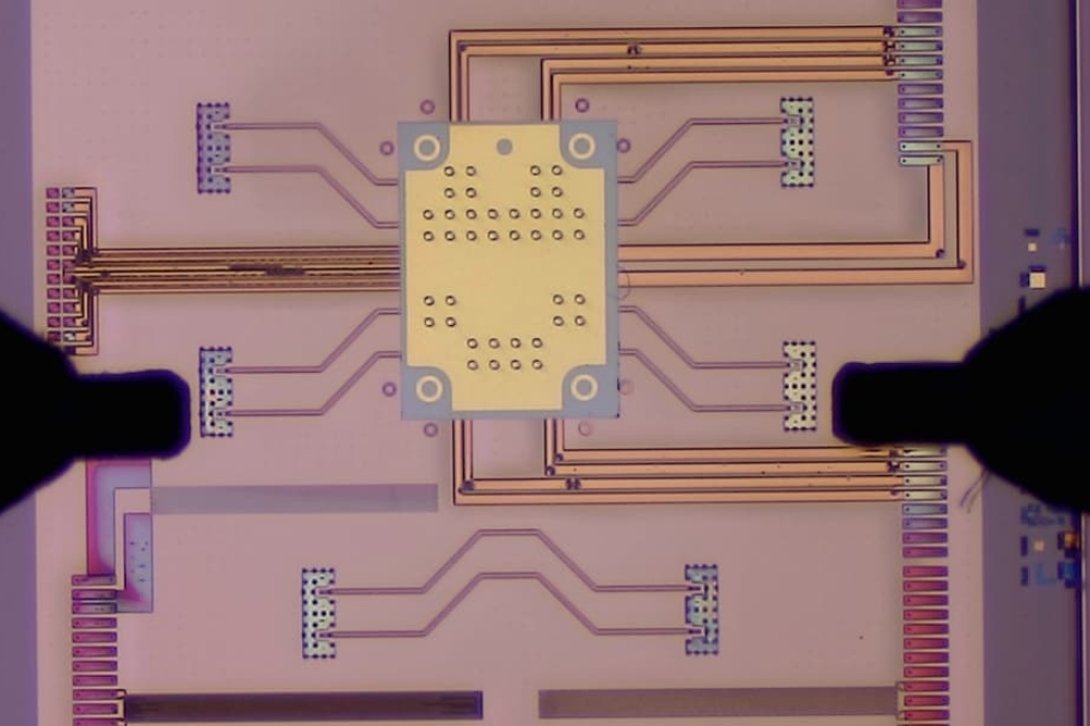
In a new paper titled “Electro-Optic Tuning in Composite Silicon Photonics Based on Ferroionic 2D Materials” published in Nature Light Science & Application, the team of scientists, led by research scientist Ghada Dushaq, and associate professor of electrical engineering and director of PRL Lab Mahmoud Rasras, say they have demonstrated a novel avenue for active light manipulation through the utilisation of ferroionic, 2D material CuCrP2S6 (CCPS). By integrating first-of-their-kind, two-dimensional and atomically thin materials into minuscule ring structures on silicon chips, the researchers add that they have enhanced the efficiency and compactness of the device.
According to the scientists, when integrated onto silicon optical devices, these 2D materials exhibit a remarkable ability to finely tune the optical properties of the transmitted signal without any attenuation. This technique has the potential to revolutionise environmental sensing, optical imaging, and neuromorphic computing, where light sensitivity is key.
“This innovation offers precise control over the refractive index, while simultaneously minimising optical losses, enhancing modulation efficiency, and reducing the footprint, rendering it suitable for next-generation optoelectronics,” said Rasras. “There is an exciting range of potential applications, from phased arrays and optical switching to use in environmental sensing and metrology, optical imaging systems, and neuromorphic systems in light-sensitive artificial synapses.”


