
Luceda Photonics releases new Test Design Kit
The company is aiming to help PIC designers build in testing requirements from the outset with its first Test Design Kit, which has already been used with VLC Photonics’ automated testing services
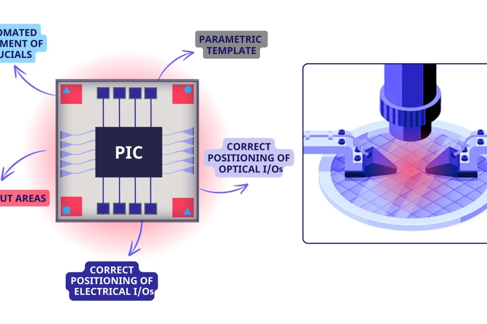
Luceda Photonics has announced that it has launched the first Test Design Kit (TDK) for the Luceda Photonics Design Platform. TDKs enable PIC designers to test their designs efficiently and cost-effectively after fabrication. This includes parametric templates, compatible with the processes of any foundry, where a set of layout rules is defined in alignment with the capabilities of specific test houses.
The concept of “design for test” plays a crucial role in standardising the testing process for PICs. Essentially, it means that designers create their circuits while considering test requirements and restrictions right from the outset. However, implementing this concept is easier said than done. When combining requirements from foundries with those of testing partners, potential pitfalls can easily arise.
According to Luceda, its TDKs provide design rules and layout guidelines that allow designers to position the input and output ports of their circuits, both optical and electrical, in a way that is compatible with standard automated testing routines. The company says that this shift in mindset encourages designers to consider testing as an integral part of the design process, rather than an afterthought, and allows test houses to reduce engineering costs for the measurement setups and hence to speed up and lower the cost of the test campaigns.
“By using a TDK alongside a foundry PDK from the start of the design flow, designers can now easily create PIC designs that are naturally compatible with automated testing routines, eliminating the need for investing in custom and costly testing solutions,” said Chiara Alessandri, Product Marketing Manager at Luceda Photonics. “As a design software provider, we strongly believe it is our role to empower designers to create first-time-right designs that can be tested easily.”
Photonic design and test house VLC Photonics was the first company to implement such a TDK for their characterisation capabilities.
“The possibility for any designer to easily load our test layout rules seamlessly into Luceda IPKISS, and to do it parametrically for more than 30 foundry PDKs, is a great step forward”, said Iñigo Artundo, CEO of the company. “With this, any PIC development can mitigate the risk and lower both time and cost when moving to characterisation, after the fabrication is completed. This allows to reduce cycle times, crucial in any project or product development.”


