Luceda Photonics and Alter Technology collaborate on PIC assembly

The companies have introduced an Assembly Design Kit to help PIC designers using Luceda’s software to consider packaging from the start, designing for manufacturability and reducing time to market and development costs for new products
Luceda Photonics has announced that it is collaborating with Alter Technology to introduce the Assembly Design Kit (ADK) for Alter’s precision assembly services dedicated to PICs. The company says this partnership represents an important milestone towards enabling Luceda and Alter’s customers to design for efficient packaging – a critical step in bringing manufacturable PIC designs to market.
According to Luceda, the Alter ADK seamlessly integrates with the Luceda Photonics Design Platform, allowing designers to create PICs using Luceda’s IPKISS software, all while considering packaging rules and constraints right from the start. The company adds that this integrated approach reduces development and manufacturing costs, accelerating time to market and reducing risks associated with new product development.
“At Luceda Photonics, we believe that bringing awareness of assembly rules to the beginning of the design cycle is a game-changer for photonic integrated circuit design,” said Pieter Dumon, CTO at Luceda Photonics. “By considering packaging rules from the outset, we empower our customers to bring efficient and manufacturable designs to market faster. The integration of Alter Technology’s packaging rules in the Luceda Photonics Design Platform represents a significant step forward in that direction.”
Matt Booker, Commercial Director at Alter UK, added: “Co-design at the outset enables our customers to target a robust and deployable packaging platform, with a fast route to market. They can also avoid most of the high NRE and long development cycle usually associated with customised photonics packaging solutions.”
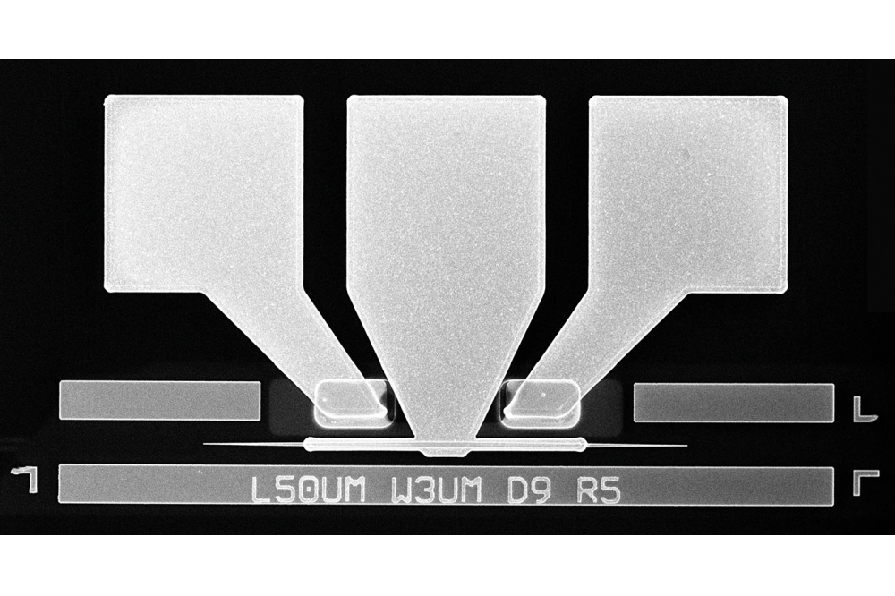
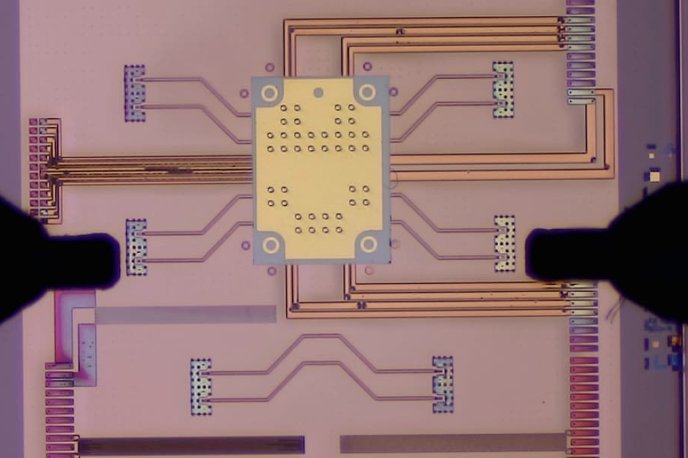
The Luceda ADK for Alter Technology features a packaging template, suitable for silicon and indium phosphide PICs, to correctly place electrical and optical inputs and outputs on the photonic chip. This includes placement rules and specifications for DC and RF bondpads, and automatic placement of fibre loops for optical packaging.
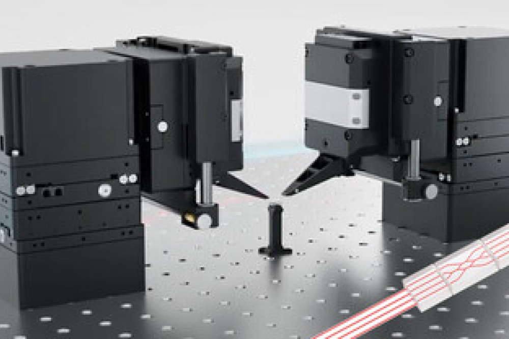
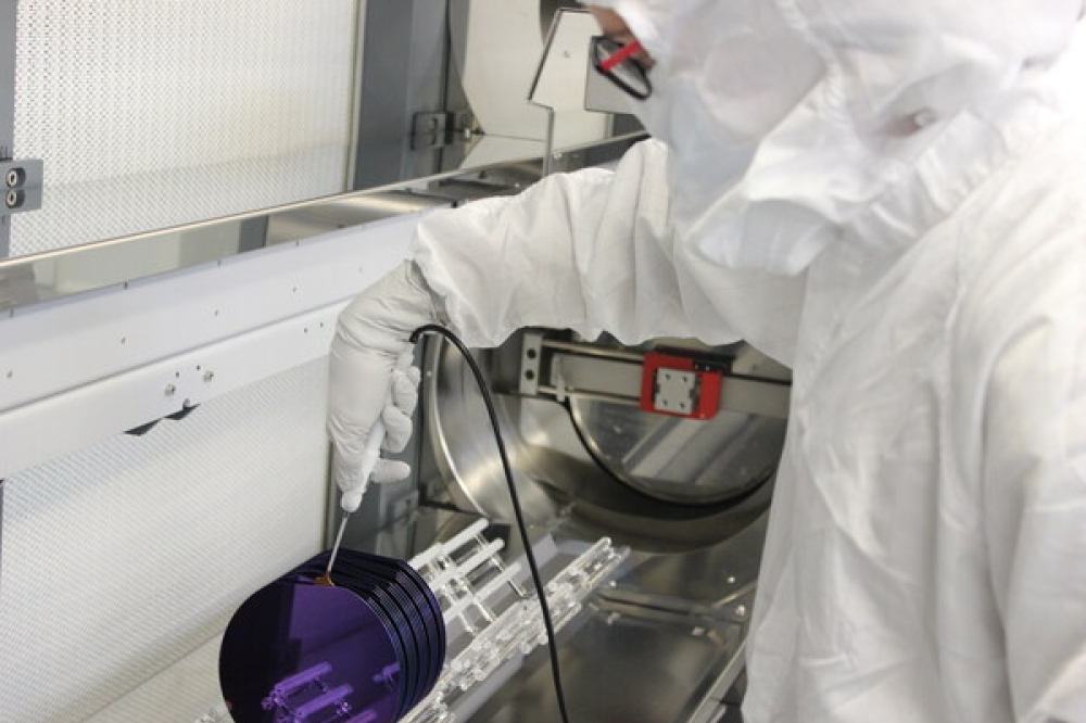
Alter’s optical packaging technology includes: multi-channel optical fibre array alignment; free-space micro-optic alignment; edge coupled and grating coupled fibre align techniques; laser weld or epoxy attachment of fibres; and precision alignment and attachment of laser or photodiode chips to PIC devices. For electrical interconnection of PIC devices, Alter Technology has experience with Au ball wire bonding, Al and Au Wedge, and Ribbon bonding for RF devices.


