
New etching technique for combining electronics and photonics
Scientists from the Technische Universität Braunschweig and the Friedrich Schiller University Jena are researching porous gallium nitride for integrated electronic and photonic circuits
While computer chips are getting smaller and faster every year, combining electronics and photonics on a single chip remains a significant challenge. Although components such as micro LEDs are available as individual chips and waveguides as tiny fibre-optic cables, the materials required are rather different, making it difficult to create a harmonised chip. To address this, researchers from the Technische Universität (TU) Braunschweig and the Friedrich Schiller University Jena have teamed up to work on a new project, dubbed “OptoGaN.” This initiative looks at using a new type of etching process to create porous gallium nitride, and using this material to combine light sources and optical fibres.
The project partners want to realise three potential applications of their technology, with one start-up demonstrating each use. The scientists say this research will then benefit technologies such as waveguides, neuromorphic computers, and the Quantum Valley Lower Saxony‘s ion trap quantum computer. At the same time, the newly founded Nitride Technology Centre (NTC) at TU Braunschweig will support the further development of nitride technology and bring it into application.
Quantum computing is one potential application of the technology. Quantum computers still need large laser systems to manipulate their ions, but, if more and more quantum bits are to be calculated together in the computer, this laser system must be shrunk down to the size of a chip or smaller. However, the standard material silicon dioxide for waveguides on chips absorbs precisely the critical wavelengths of light. The porous gallium nitride could offer an alternative here and bring the customised light to the individual ion with minimal loss.
The porous semiconductor is based on a new selective etching process, by which the researchers create elongated, air-filled channels – pores – in the gallium nitride structures. This even makes three-dimensional waveguides with complex optical light guidance conceivable. As gallium nitride and the process are compatible with existing LED production methods, integrated electronic and photonic circuits will also be possible.
In order to realise the innovative semiconductor channels for light guidance, the researchers from Braunschweig and Jena are bringing together complementary expertise and special equipment. This is because the etching process used here has both an electronic and a chemical component. Firstly, the Braunschweig researchers produce the base material layer by layer. The semiconductor chip then travels to Jena for ion implantation. The researchers from Jena dope the chip and change its electronic properties in a targeted manner. Finally, the chip returns to Braunschweig, where the chemical etching process forms the final, porous structure.
The OptoGaN project (short for Highly integrated microphotonic modules in nitride technologies) is being funded by the Federal Ministry of Education and Research with around €600,000. It was launched in 2023 and will run for three years until October 2026.
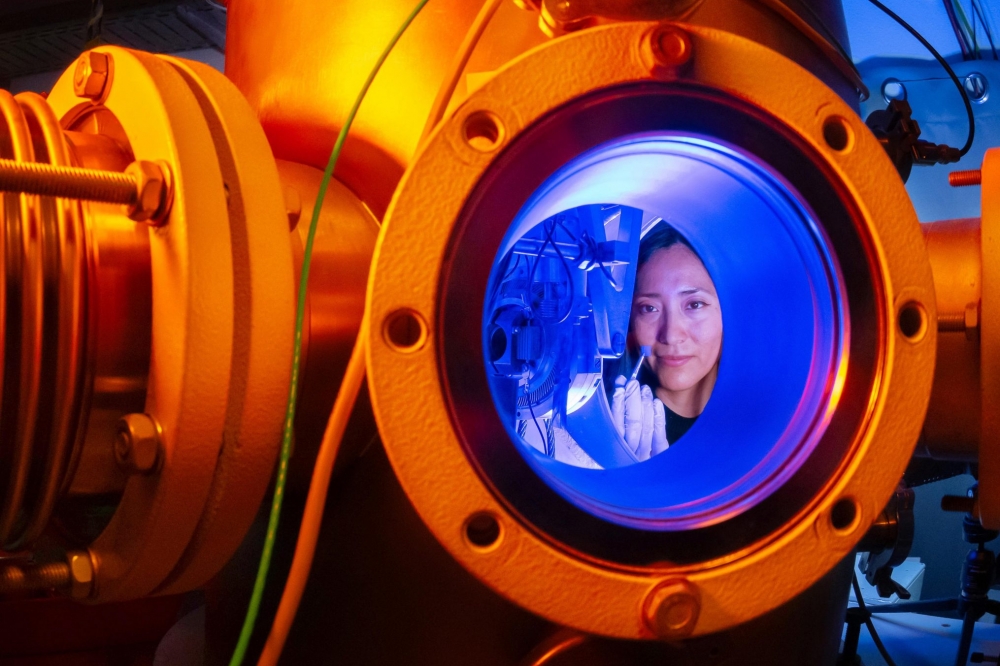
Image credit: Jens Meyer/University of Jena


