Tuneable lasers: The elusive trifecta

Integrated tuneable laser assemblies serving in the C- and O- bands
excel on three fronts by offering the unique combination of wide tuning,
fast-nanosecond switching and a narrow linewidth.
BY CAOLÁN MURPHY, SHANE DUGGAN, GAURAV JAIN, CRISTIAN VARGAS, AND DESI GUTIERREZ FROM PILOT PHOTONICS
TUNEABLE LASERS are now established as a key enabling technology in a wide range of applications, spanning various fields from optical communications to sensing.
In telecommunication infrastructure, particularly in the long-haul and metro networks, widely tuneable lasers with a low linewidth are indispensable components. When incorporated in coherent transceivers, their low linewidth enables increased data rates by supporting advanced modulation formats within dense wavelength-division multiplexing systems. The wide wavelength tuneability is a valued asset, simplifying network design and management by enabling resources to be dynamically assigned and optimised while reducing inventory requirements.
Meanwhile, in optical fibre sensing applications, such as fibre Bragg grating sensing, fast-swept tuneable lasers are used to interrogate sensors with Bragg gratings inscribed into optical fibres. These gratings reflect specific wavelengths of light, based on the strain and the temperature applied to the fibre, to create a distinctive spectral signature. When lasers offer fast switching and are widely tuneable, this enables precise and fast wavelength sweeps across the fibre Bragg grating sensor’s bandwidth to ensure real-time, accurate readings of strain or temperature.
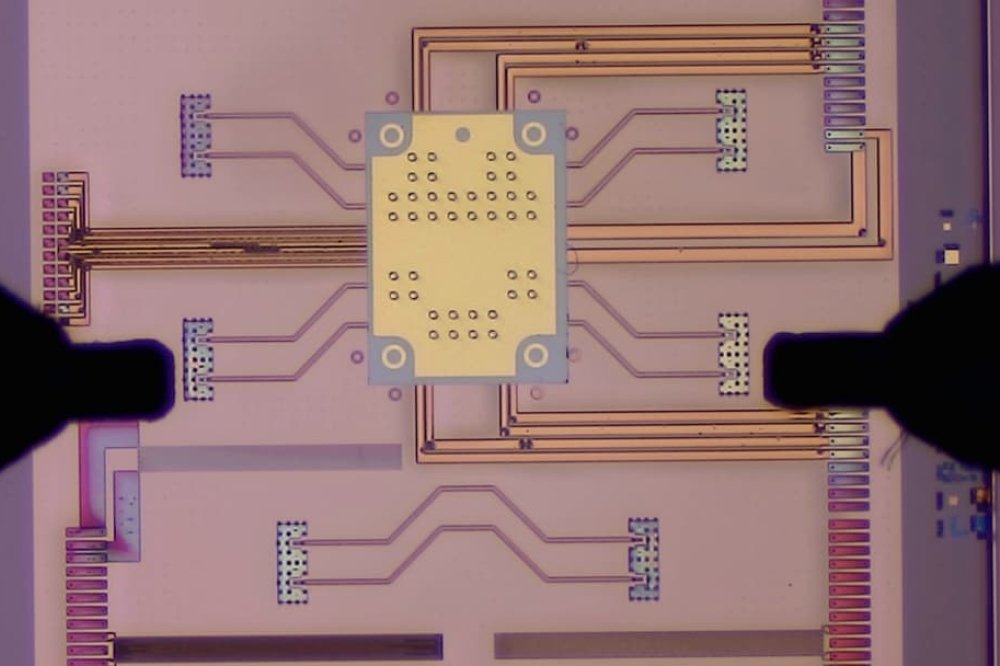
Figure 1. Tuneable laser form factor offerings: Photonic Integrated
Circuit (PIC), the laser cavity consists of a gain section providing
optical gain in either the C or O bands, two ring sections that act as
tuneable mode selectors through the Vernier effect, and a common phase
section to allow finer tuning of the laser cavity mode; 14-pin butterfly
package; OEM benchtop unit; nano-integrated tuneable laser assembly
package.
Fast tuneable lasers have also played a key role in the development of many optical switching architectures, involving rapid adjustments to the laser wavelength to quickly switch or route optical traffic without having to convert signals to the electronic form.
There is no doubt that the versatility of the tuneable laser has enabled widespread applications. However, today’s commercially available widely tuneable lasers still fall short in some areas. In particular, they struggle to serve in applications requiring phase-sensitivity and very fast-switching/sweeping.
For instance, for frequency-modulated continuous-wave lidar, a cutting-edge technology in autonomous vehicles and remote sensing, they are not adept at providing the low linewidth and ultra-fast sweeping capabilities needed to precisely measure distances and velocities. Additionally, in systems that employ coherent optical time-domain reflectometry and optical frequency-domain reflectometry, rapid, phase-sensitive tuning is critical for accurate detection of disturbances or variations along the optical fibre, or for other devices under test. If optical packet or optical burst systems are to re-emerge, they will have to align with the demands of today’s high-speed data transmission, which requires not only very fast wavelength switching, but the ability to handle phase-sensitive modulation formats.
The three desirable characteristics for tuneable lasers, as well as the
typical design rules required to achieve them. Few designs are able to
achieve the combination of wide tunability, fast switching and narrow
linewidth.
Unfortunately, today’s widely tuneable semiconductor lasers are not great allrounders. Typically, they offer either a narrow linewidth or fast tuning – but not both. An example is the sampled-grating distributed Bragg reflector laser, which is capable of tuning across tens of nanometres using the Vernier tuning effect, thanks to a current-injection-based tuning mechanism that enables swift optical switching. However, this comes at the expense of increased phase noise and broader linewidths, rendering this design unsuitable for the aforementioned applications.
The alternative is to make use of an equivalent thermally tuned laser. This class of laser is capable of realising similar tuning ranges, while boasting low linewidths. However, fast electronic tuning is sacrificed. Similarly, SiN ring-resonator-based devices major in ultra-low linewidths via thermal tuning, but dramatically reduce switching speeds, also limiting usage in these applications.
Figure 2. Example of Light-Current (L-I) and
Current-Voltage (I-V) curves. The C-band device has a threshold current
of 30 mA, while the O-band device has a higher threshold of 50 mA.
However, a higher slope efficiency in the O-band device results in a
higher optical power at a nominal current of 100 mA. The O-band device
is expected to operate at a higher voltage due to the wider bandgap
required to generate light in the O-band.
The elusive combination of a broad tuning range, narrow linewidth and either rapid switching or sweeping, has been a long-standing industrial challenge. Breaking through this impasse to fulfil the elusive trifecta is our team at Pilot Photonics of Dublin, Ireland. Working with the InP foundry Smart Photonics, we are trailblazing lasers that blend all three desirable properties.
Available in both the C-band and O-band, our ground-breaking lasers unlock new possibilities across a spectrum of applications, from lidar to optical coherence tomography, dense wavelength division multiplexing, coherent optical communication, distributed fibre sensing, gas sensing, sensor interrogation, fibre optic testing, and optical switching. That’s a vast and varied range of applications.
Currently available in a 14-pin butterfly package, or instrument formfactor, our nano-integrated tuneable laser assembly that’s targeting high-volume communication applications will be released later this year (see Figure 1). Each package features an integrated feedback control, based on wavelength-meter and wavelength-locker systems. Incorporated in the wavelength meter are a linear filter and a photodetector, employed to estimate the current lasing wavelength, and a wavelength locker that consists of an etalon and photodetector – this allows the monitoring of the wavelength on a 50 GHz or 200 GHz grid. Combining the two feedback systems ensures closed-loop control of the device during operation.
Figure 3. Mode maps generated by sweeping voltages to the two ring
tuners (with current into the gain section and voltage to the phase
section held fixed). The wavelength map on the left shows a series of
discrete regions, in which wavelength is relatively fixed (the modes). A
map of the side-mode suppression ratio (SMSR) on the right indicates
regions where only a single lasing mode is dominating. Regions of low
SMSR (<30 dB) indicate a transition between modes (mode hops).
Monolithic dual ring architecture
Our lasers are fabricated on a monolithic InP chip utilising an active-passive integration scheme. The design employs a looped cavity with a gain section that provides optical gain, and two ring-resonators that act as transmission filters for wavelength selectivity through Vernier tuning (see Figure 1 for details). The ring-resonators, which are electro-optically tuned through reverse-bias voltage application, have remarkably low dark currents – they are in the low milliampere range. These low-power, low-current passive tuning sections are crucial to realising optimum device performance. Low dark currents minimise linewidth broadening and device power consumption, while low heat dissipation in the tuning sections eradicates troublesome slow thermal transients. Thanks to these strengths, we realise nanosecond-level switching speeds.
Wide-band tuning is achieved with the Vernier effect. The desired emission wavelength is selected through the overlap of the transmission filters of two ring resonators, each with a slightly different free spectral range. These filters produce a series of discrete lasing modes when one ring is tuned relative to the other. A long phase tuning section in the large outer loop provides fine tuning of the cavity mode within the ring filter envelope.
One of the benefits of the Vernier mechanism is that it opens up an avenue for ‘step-and-sweep’ style tuning, important for many frequency-modulated continuous-wave lidar systems. The idea behind step-and-sweep is as follows: tune the rings relative to each other to produce a series of discontinuous hops between ring modes (step), before ramping the phase section with a defined signal to produce
a continuous change in frequency (sweep) within each of these modes.
To increase the output power, we integrate a semiconductor optical amplifier. This boosts the output to 30 mW (+14 dBm), with further increases expected. The addition of this amplifier also enables output power stabilisation, thanks to the possibility to readjust the output independently from the cavity.
Figure 4.A set of individual spectra taken across the optical O-band. Each line represents a discrete tuning mode of the laser.
We have recorded the characteristics of our original C-band designs and our more recent designs in the O-band. By plotting light-current-voltage curves, we have determined the likes of lasing threshold, slope efficiency and power consumption. Our C-band devices, which do not include a semiconductor optical amplifier, produce an optical output power of 0.5-1.0 mW. O-band variants have a higher lasing threshold but compensate with higher optical powers. Without the addition of the amplifier, the output power is 1.0-2.5 mW (see Figure 2). During normal operation, the devices typically consume 130 mW, excluding the power drawn by the thermo-electric cooler.
For the spectral characterisation of our devices, we use ‘mode-maps’. These two-dimensional maps represent the tuning space of the laser – in other words, the lasing wavelengths produced by every combination of voltages supplied to the two rings on a two-dimensional grid (see Figure 3 for more details). These wavelength maps feature a series of discrete regions (modes), in which the wavelength varies continuously. Crossing a boundary between the modes results in a wavelength discontinuity, known as a mode-hop.
Another important quantity to record on these maps is the side-mode suppression ratio. The value for this ratio offers an insight into the competing modes in the optical spectrum – when this ratio is low, that’s below 30 dB, a mode hop is about to occur.
These maps can also be used to determine suitable operating points for the laser under step-and-sweep operation, and to identify optical switching pairs.
By sweeping the phase section, the tuning space for these maps expands into the third dimension, providing a more comprehensive characterisation. However, such maps are much more difficult to visualise.
We have used mode maps to determine the tuning range for our lasers. It’s nearly 30 nm in the O-band and over 35 nm in the C-band.
Once a suitable set of operating points are extracted from the mode maps, it is possible to measure the optical switching speed (see Figure 4). To validate the nano-second switching speeds expected from the device, we use a simple frequency discrimination technique. By supplying one or more tuners with a low-frequency square-wave signal, with a suitable amplitude to produce a hop between two modes, we produce a repetitive optical switching signal. Following photodetection, this produces an electrical signal of the same frequency as the input signal, with the rise/fall time being equal to the optical switching time.
Figure 5. A switching speed measurement taken using a frequency
discriminator. The square-wave voltage applied to one of the rings (a)
produces two complimentary optical signals (b), (c) – one for when the
optical filter is centred on each of the two switching modes. The
switching time is equal to the fall time of the optical signal, measured
to be 3.6 ns.
Using this method, we have recorded switching speeds consistently below 10 ns, and as short as 3.6 ns (see Figure 5 for more details). That’s up to three orders of magnitude faster than typical lasers based on thermal tuning.
Having established that our laser is fast, the next crucial question is this: what is its noise characteristics, and in particular its linewidth? To answer this, we have used a delayed self-heterodyne technique to measure the linewidth, obtaining values from 400 kHz down to 100 kHz in both C- and O-band devices (see Figure 6). While this is still broader than most external-cavity-type lasers, it is a significant improvement over fast-tuning sampled-grating distributed Bragg reflector lasers, which would be expected to have linewidths in the megahertz range. The level of noise indicates that our devices are suitable for coherent transmission applications. With our collaborators in Dublin City University, we have proven this, realising 480 Gbit/s 16-QAM transmission over 25 km of optical fibre. This result demonstrates the capability of our lasers for serving in optical access, metro, and data-centre networks.
Figure 6. Spectrum fitted to a Voigt profile. Lorentzian linewidths as low as 100 kHz have been recorded.
Future impact
According to the Tunable Laser Market Research Report, published by Market Research Community, the tuneable laser market is projected to grow by 8.8 percent per year from now to 2030, by which time it will climb to $23.2 billion. Helping to fuel this growth will be improvements to the technology, such as those just described, that will enable new applications, enhance existing ones and have far-reaching impacts on healthcare, telecommunications, transportation and many other sectors.
There is no doubt that producing tuneable lasers that combine wide tunability with a low linewidth and either ultra-fast switching or sweeping is an important step forward. In the optical networking field, it enables new datacentre switching architectures that promise to trim power consumption by keeping as much traffic in the optical domain as possible, and only converting to the electronic domain the traffic that is necessary.
The evolution of telecom protocols like 5G and the anticipated 6G necessitate ever-faster laser switching speeds, wide tunability, and low latency – all are required to ensure the seamless communication that’s essential for our connected future. Moreover, the impact of lasers that excel on all these three fronts extends to advancements in metrology techniques, benefiting applications such as lidar, healthcare diagnostics and industrial sensing, where phase sensitivity and speed are critical.
Key to the potential of this unique laser is its monolithic integration. Thanks to this, it can be manufactured at wafer scale using today’s InP processing techniques, ensuring a cost profile that is compatible with the very high-volume applications envisaged today and into the future.
Further reading
† S. Andreou et al. “Electro-Optic Tuning of a Monolithically Integrated Widely Tuneable InP Laser with Free-Running and Stabilized Operation,” J. Light. Technol. 38 1887 (2020)
† G. Jain et al. “Widely tunable C-band laser and module with fast tuning and narrow linewidth,” Proc. SPIE 12424 Integrated Optics: Devices, Materials, and Technologies XXVII, 124241M (2023)
† C. Murphy et al. “Widely Tunable O-band Laser with Narrow Linewidth, Fast Switching Speed and an Integrated SOA”, ECOC 2023, Th.B.4.2.
† M. Troncoso-Costas et al. “Experimental demonstration of 480 Gbit/s coherent transmission using a nanosecond switching tuneable laser”, Opt. Commun. 554 130164 (2024)


