Three ways photonics can catalyse hardware evolution for datacoms

As the computing industry faces ever-growing demands for higher speeds,
photonic technologies can facilitate the necessary hardware evolution,
through hybrid integration, chip disaggregation, and enabling 200G per
lane.
BY SURESH VENKATESAN, CHIEF EXECUTIVE OFFICER, POET TECHNOLOGIES
OF THE MANY THINGS artificial intelligence has upended, the microchips industry may be the sector that has seen the most disruption. AI applications are gluttonous for speed and power, and, as the computing industry has raced to meet the demand, it has become apparent that existing solutions will not suffice. There is a growing sense of urgency across the industry as it becomes increasingly clear that optical interconnects enable large-scale AI compute and other data-intensive workloads to operate at bandwidths, energy efficiencies, and latencies that are unachievable through today’s electrical-based interconnect technology.
Sixty-plus years after engineers commercialised the first monolithic integrated circuit chip, the explosion of AI and the insatiable demand of hyperscale datacentres for more bandwidth have offered a remarkable opportunity for chipmakers to move beyond traditional solutions in a dramatic way. While materials such as indium phosphide and gallium arsenide have been used in commercial applications for decades, the growth of material-agnostic optical platforms has presented the chance to transition from “silicon-only” to “silicon-plus” designs.
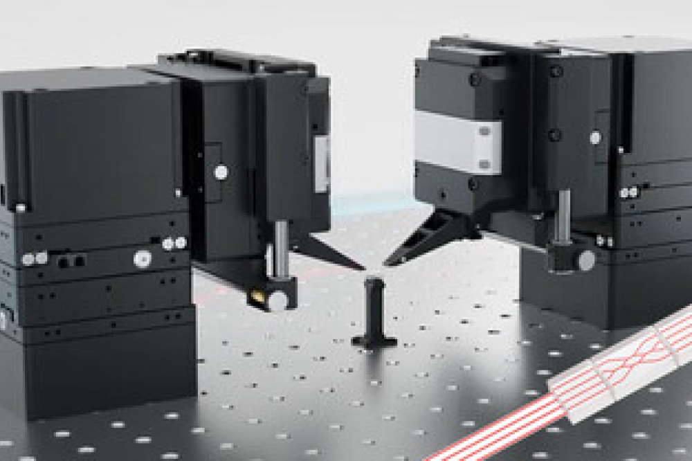
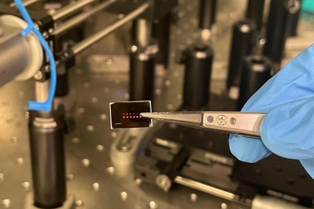
The POET Technologies O-Band LightBar, shown with lasers assembled, is
developed to help AI manufacturers bring next-generation products to the
market.
Whereas the absolute need for silicon will never wane, the slowing of Moore’s law has opened the door to “augmented silicon” technologies.
These approaches aim to enhance silicon’s innate capabilities and advantages through the incorporation of new materials (germanium, indium phosphide), new architectures (chiplet and hybrid system partitioning), and 3D packaging and assembly. That’s the reality many manufacturers and industry observers have recognised so far this decade.
One of the ascendent technologies is photonics, with many companies currently in the midst of identifying optical computing solutions that will
drive the next generation of device manufacturing.
The following are three key areas where photonics — which was once a boutique niche — is positioned to be the catalyst for large-scale growth in hardware applications for AI and hyperscale datacentres.
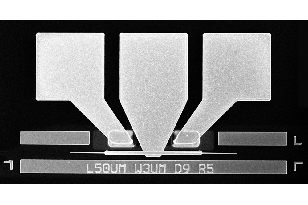
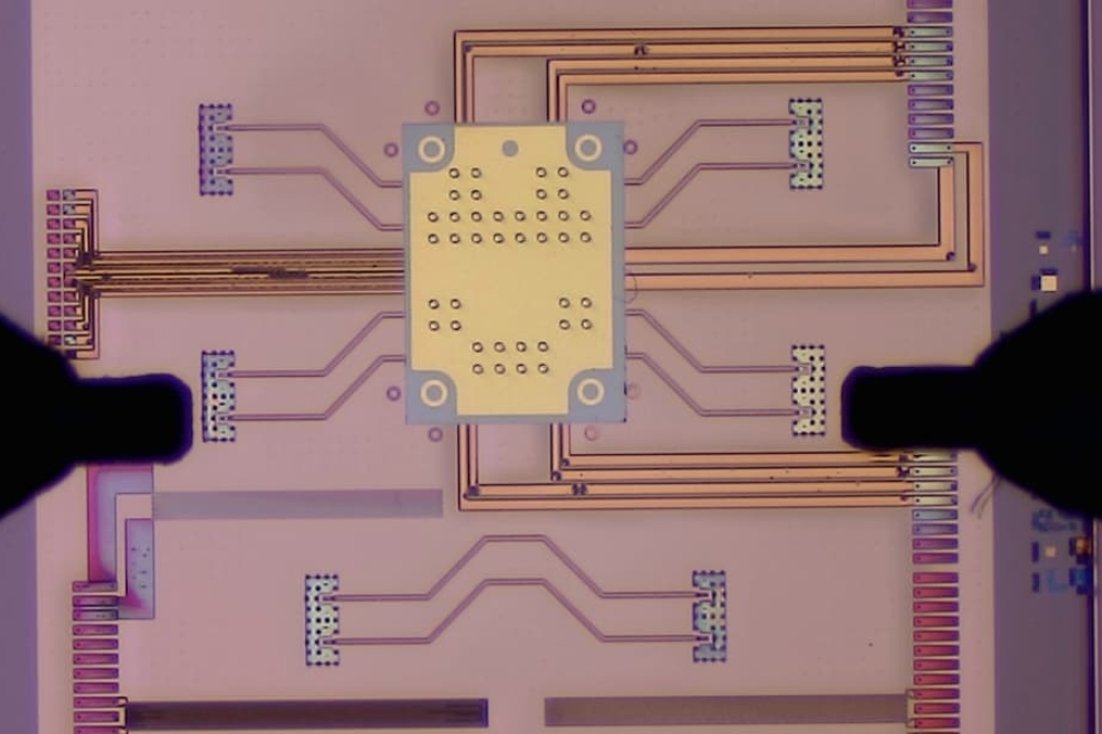
The POET Technologies 400G Infinity Transmit Chiplet demonstrates the flexibility of the company’s optical interposer platform
Hybrid Integration
With a hybrid-integration approach to wafer-scale chip design, developers can assure those manufacturers who have built their entire operations around silicon that the coming wave of product design will have several familiar pieces. In this way, hybrid integration allows for a seamless transition to future paradigms.
At POET Technologies, our “semiconductorisation of photonics” approach is a form of hybrid integration. That term is meant to underscore the intention behind our designs: to make it as straightforward as possible for the semiconductor industry to move to photonics-first solutions that are material agnostic. Our elegant design eliminates dozens of parts because we rely on passively attached optical components to move data, leveraging the broad semiconductor industry’s investments in advanced packaging technology.
Based on a “silicon for photonics” interposer platform, POET’s products offer manufacturers a critical piece of the puzzle of achieving high integration, especially for 1.6T, 3.2T, and beyond. With its “silicon for photonics” hybrid integration approach, POET is focused on addressing the shortcomings of more conventional silicon photonics solutions. To this end, POET’s technology includes features like passive alignments, low-loss multi-layer waveguides, and integrated optical passives like multiplexers and de-multiplexers that have the flexibility and fungibility to address a broad range of market requirements.
Such flexibility and integration are crucial, because serial data communication channels have not been able to keep pace with growing bandwidth. The number of communications lanes increases as data rates increase. Those manufacturers who rely on conventional discrete assembly are challenged to economically deploy products that perform consistently within eight-channel architecture – which is needed for 800G speeds – and are incapable of accommodating 16-channel lanes – which is necessary for 1.6T and 3.2T, the speeds of the future.
POET achieves 16-lane capability by using 3D assembly techniques and stacked non-interacting waveguides. It’s a simplified process that drives data communications at unprecedented speeds.
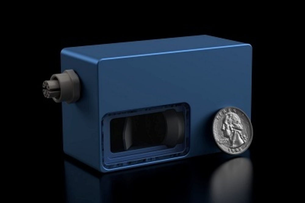
The POET Technologies 800G solution includes 2xFR4 receive optical engines with a trans-impedance amplifier and photodiodes.
200G per lane
Moving data simultaneously through more lanes is one way that photonics brings superior capability to the market. Another is its ability to increase the speed that can go through each of those lanes. Conventional speeds are currently 100G per lane but photonics can operate at 200G per lane, busting the bottlenecks that cause latency and high power consumption. At 200G per lane, AI and hyperscale datacentres and cloud networks can surge towards new capacity limits.
Among the giants touting the merits of 200G per lane solutions is Broadcom, which demonstrated an optical transmission link using that configuration at OFC 2023. “The demo not only validated the feasibility of 200G per lane optical links for datacentre networking, but also reassured the ecosystem that 1.6T optical modules can cost-effectively be deployed to address the growing bandwidth demands in datacentres supporting AI applications and workloads,” wrote the company’s master engineer Khanh Lam.
A key component needed to achieve 200G per lane is an externally modulated laser (EML). Already, more than 90% of 800G modules in production today use EMLs, which present the primary path to 200G per lane solutions. The performance of EMLs and the industry trust they have attained are reasons why POET has retooled its optical interposer platform to include both EML and DML (directly modulated laser) solutions.
Disaggregation
“Chip disaggregation, or chiplets, offers an alternative to the traditional monolithic SoC scaling approach. Aggregating multiple chiplets to perform the function of a single monolithic IC de-risks the overall system by reducing complexity and increasing yields,” writes chip producer Rambus.
With the conventional processor-centric computing architecture and copper interconnects, the chips based on 3 nm technology that have dominated semiconductor design for decades are approaching their physical limitations. The necessity for faster data transmission has gone beyond what these chips can capably deliver. As a result, disaggregation is going to push the need for photonic connectivity. It’s already happening at Google, whose AI servers are exploiting disaggregation to connect to networks with 800G transceivers — making the search-engine leader the first company to commit to using that speed for its datacentres.
Products such as the POET Infinity chiplet, and the family of engines built from them, provide an answer for pluggable transceiver and module designs. The Infinity, a 400G transmitter chiplet, can be configured in a daisy-chain architecture to reach speeds of 800G (2x400G chiplets), 1.6T (4x400G), and beyond. As with all products built from the POET Optical Interposer, the Infinity chiplet includes a monolithically integrated multiplexer, and eliminates wire bonds and active alignments of components.
Photonics-first innovations such as those being introduced to the market by POET and other companies promise to pave a new path forward in the AI era. The industry is in the middle of an important stage as it develops new processes to power computing performance. The platforms and products that are adopted now are likely to be the de facto choices for chipmakers for decades to come.


