Lumentum expands Caswell fab, reflecting company-wide plans for growth
Lumentum is due to complete a 25 percent expansion of its wafer fab at Caswell Science and Technology Park in April this year. Editor, Laura Hiscott visited the facility to learn how these activities fit into the company’s wider strategy for growth.
In the heart of the UK countryside, surrounded by fields and more than half an hour’s drive from the nearest train station, is a large campus where around 400 people gather to work each day. Caswell Science and Technology Park certainly seems far from the hustle and bustle of a city, but its remote location belies the integral role it plays in the modern world.
The site is a 3-inch indium phosphide fab belonging to the global photonics company Lumentum, and it manufactures photonic chips for data transmission over optical fibres – essential components underpinning the internet and our digital lives.
Caswell’s rural setting is a historical legacy – it was originally developed during the Second World War, when its founder was encouraged to build it far away from London and the risk of air raids. Today, however, being surrounded by empty fields offers an entirely different advantage: there is plenty of space to grow. And Lumentum is taking full advantage of that potential.
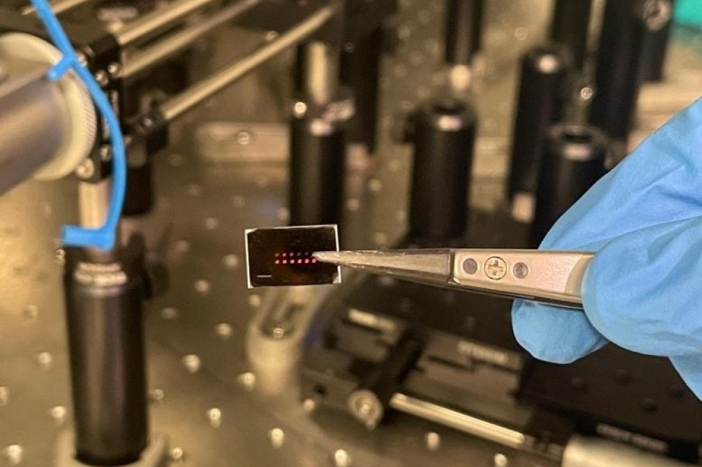
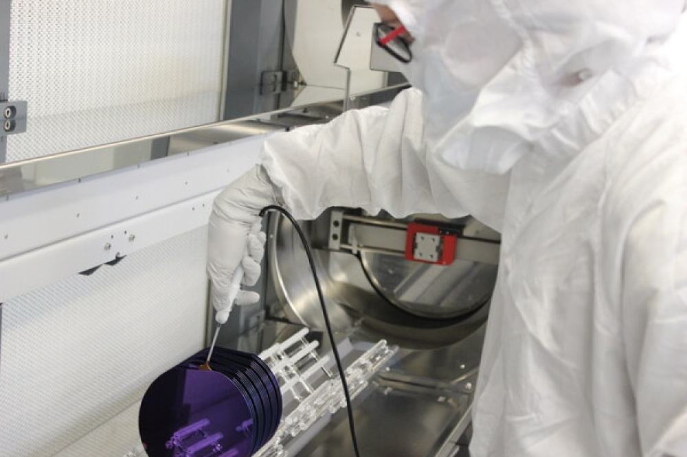
Caswell manufactures indium phosphide optical modulator chips, which can be found in many of Lumentum’s products.
After gaining Caswell as part of its acquisition of optical manufacturing company Oclaro in 2018, Lumentum initially leased the land it was situated on. But in September 2023, the company bought the land, and is now investing in significant upgrades. Chief among these is a major expansion of the cleanroom, which is due to be completed this spring, increasing its size and production capacity by 25 percent.
These actions affirm the facility’s value to Lumentum, and its key role in the company’s plans moving forward. “Lumentum’s investment in equipment, infrastructure, and people at Caswell will be key to the company’s continued success,” says Sal Pavone, vice president of operations. “We are committed to make this the centre of excellence for the manufacture of photonic products.
Many of our key products are manufactured at Caswell and are dependent on the leading-edge technology that is developed here on site.”
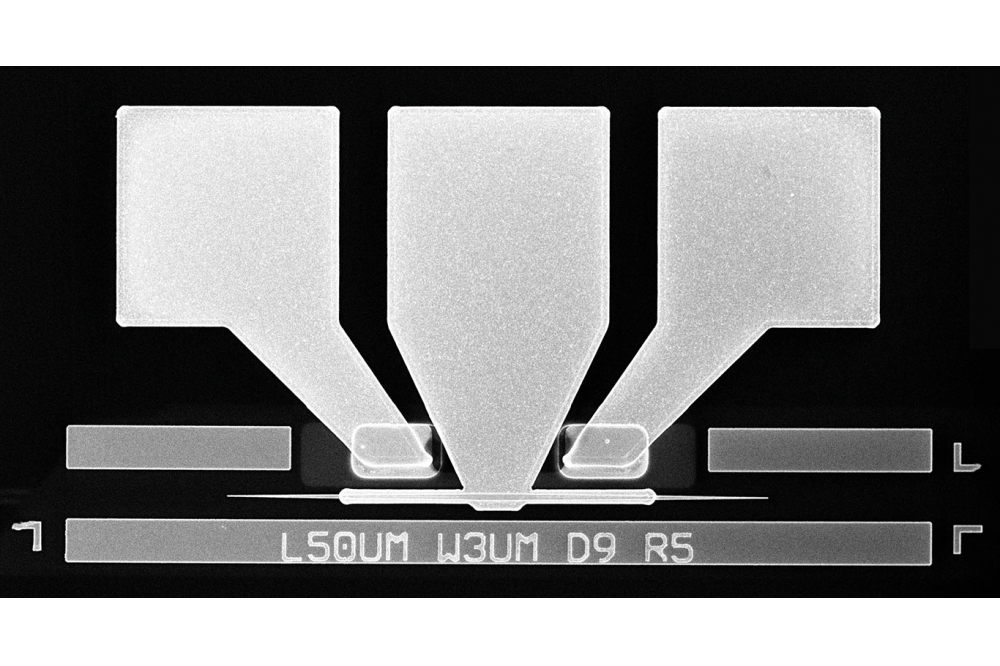
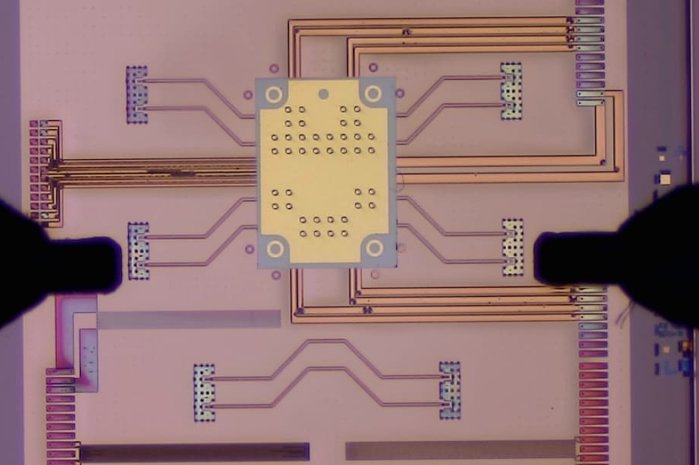
Indeed, Lumentum’s 800G ZR+ and 400G ZR+ 0 dBm transceivers, and 130+ GBaud components and Smart TROSAs, which were on display at ECOC 2023 in Glasgow last year, all contain chips from Caswell. They include, for example, InP modulator chips that incorporate multiple Mach-Zehnder modulators and on-board optical amplifiers, as well as on-chip photodetectors for monitoring and control functions.
Paul Johnson, senior director of product line management for cloud and networking, points out that these chips offer several key advantages of InP over other PIC platforms, enabling differentiated performance for cloud and networking. “They have very high-speed capability beyond 100 GHz electro-optic bandwidth, optical light generation and amplification, and ease of integration of these capabilities,” he says. “We can combine the best of laser and modulator or receiver performance without compromise, enabling optical fibre data transmission at 800G per fibre or higher, a 1,000 times greater capacity than the typical fibre-to-the-home connection.”
Global network
Caswell is one of eight manufacturing facilities that Lumentum operates across three continents, with many more non-fab sites around the world. This global presence means that the company can be close to all its various customers. While different locations may have a different focus, they all perform several functions, and employees at different sites work together towards the company’s overall goals.
An important advantage of having the same products manufactured at multiple sites is the redundancy and the associated supply chain security that this distributed structure offers. Additionally, forming teams of people across the different locations, rather than limiting them to employees at the same site, widens the possibilities for finding the optimal combination of skills and perspectives needed for a particular project.
The chips made at Caswell are generally transferred to Lumentum’s other facilities for packaging into final products. However, in addition to producing photonic chips, the site also plays an active role in developing the company’s future-generation products. For this reason, it has a smaller-scale assembly line to enable rapid development of prototypes.
There are R&D teams based locally working on improving chip designs, process integration and optical sub-assemblies (OSA). Caswell also has R&D teams researching the integration of chips into larger components and developing the test infrastructure. “The need for innovation to move to higher baud rates doesn’t stop,” comments Lloyd Langley, vice president of R&D. “I remember introducing products with lasers operating at 10G many years ago. Now we have products operating at 130 Gbaud, and advanced technology work aimed at 260 Gbaud for 1.6T per laser applications. These higher rates are operating with RF signals exceeding 100 GHz. In addition, other aspects such as minimising power consumption are an important consideration.”
Company-wide growth
Besides affirming Lumentum’s investment in the region, the expansions underway at Caswell also reflect wider growth across the company. Last year, for example, it announced that it had increased manufacturing operations and R&D capabilities at its site in Slovenia, which focuses on custom optical fibres found in many Lumentum products.
Furthermore, the company has made multiple acquisitions in recent years, cementing its position as a major player in the industry, which is itself growing. Among its most notable acquisitions are two manufacturers of optical modules for datacentre interconnects: NeoPhotonics in 2022, and Cloud Light in October last year.
As Lumentum continues to grow, in terms of both its manufacturing and research capacities, it has every reason to believe that there will be demand for as much volume and as many product updates as it can deliver. After all, our modern lifestyles are hungry for higher data rates; streaming services and the rise of cloud computing were already fuelling an unwavering rise in internet traffic, even before the explosion of widely available AI and machine learning applications in the past few years. As computational workload increases continue to outstrip Moore’s Law, network bandwidth will need to expand by as much as an order of magnitude to handle all that information, and using optics can help to achieve that.
“AI is driving a need for scalable interconnect solutions within datacentres. Intra-datacentre transceivers, operating at 400G to 1.6T, will grow to be a $10 billion market by 2028,” explains Johnson. “The addition of Cloud Light to Lumentum helps us address that demand. As a combined company, we believe we can bring advantages such as first-to-market high-speed transceivers customised for the hyperscale market, utilising in-house manufacturing for lowest cost at scale, with the security of supply that the market requires.”
As the industry sets its sights on securing bandwidths of 800G, and moving towards 1.6T, Caswell and Lumentum are striving to stay ahead of the game in providing the supporting infrastructure. “Our process and design teams work at the cutting edge of compound semiconductor wafer manufacture and performance of PICs,” says Langley. “We have design experts in semiconductor materials, optical waveguides, very high frequency electromagnetics, test, and reliability.”
Yet, as the company and its technologies evolve, one thing looks set to remain the same. As Pavone puts it: “Caswell has been producing leading edge technology in the UK and will continue to do for years to come.”
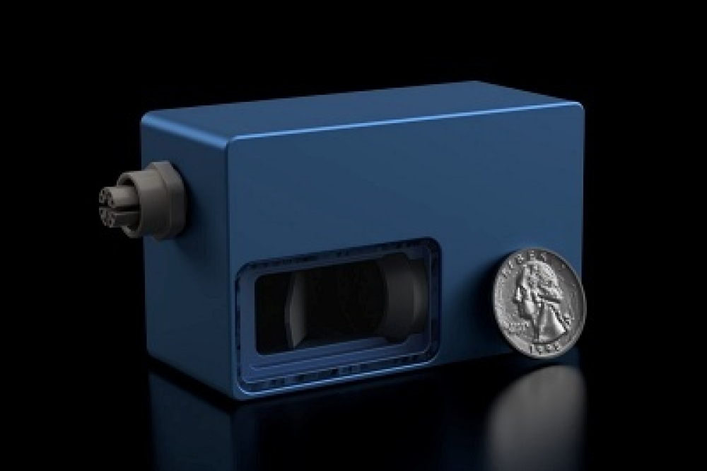
At ECOC 2023 in October last year, Lumentum introduced a 130+ GBaud Smart TROSA, which incorporates components manufactured at Caswell.
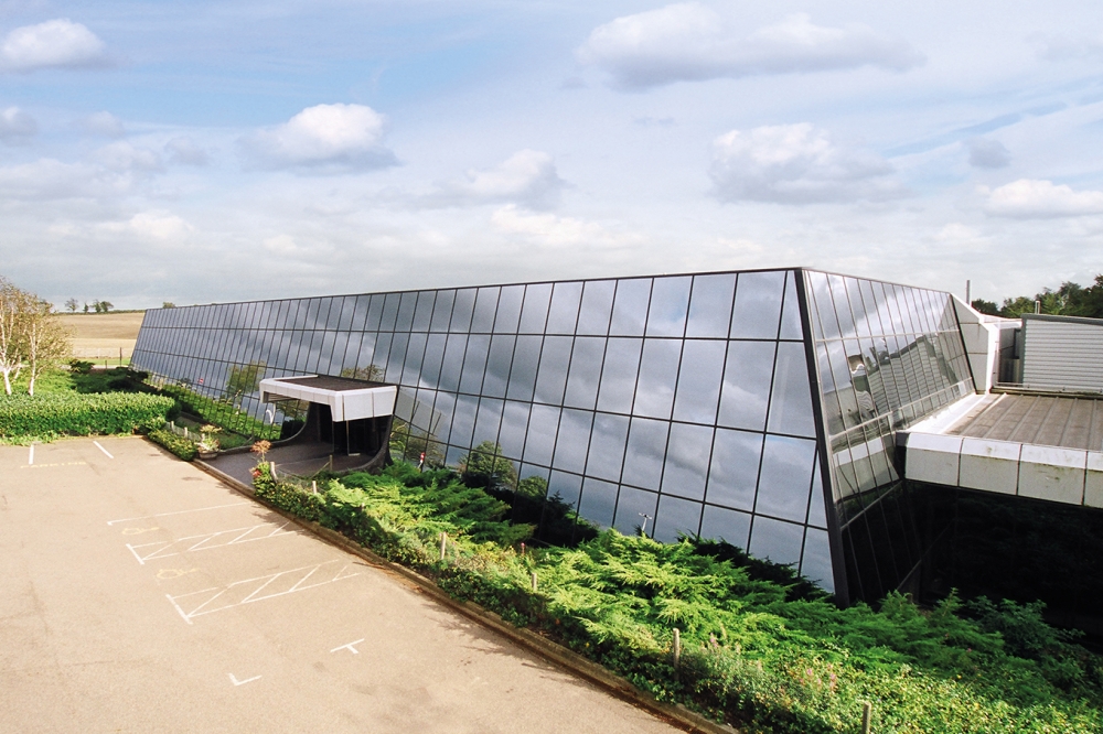
Main picture:Caswell Science and Technology Park was originally built in the
countryside to avoid aerial bombing during WWII. However, today, this
location means there is plenty of space for it to grow.


