

Moving towards polarisation-independent monolithic PICs
As datacentres race towards 200G per lane, polarisation-dependent loss and differential group delay remain significant hurdles in high-speed optical receivers. GlobalFoundries researchers have made significant progress in addressing these challenges.
BY YUSHENG BIAN, MASSIMO SORBARA, WON SUK LEE, SUJITH CHANDRAN, TAKAKO HIROKAWA, ABDELSALAM ABOKETAF, KEVIN DEZFULIAN, RYAN SPORER, KEN GIEWONT AND TED LETAVIC, GLOBALFOUNDRIES
To cope with ever-growing bandwidth demands, datacentre communication applications are transitioning to 200G PAM-4 transmission per optical wavelength (200G per lane), doubling the symbol rate to 106.25 GBaud compared with 53.125 GBaud found in 100G-per-lane systems [1, 2]. However, in 200G-per-lane systems, managing the significant impact of polarisation-dependent loss (PDL) and differential group delay (DGD) on optical receivers is increasingly challenging, particularly in optical interconnection schemes deploying monolithic silicon photonic technology.

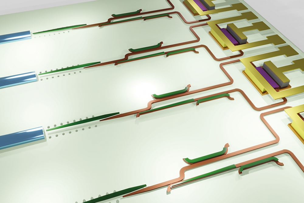
Figure 1. GlobalFoundries FotonixTM platform monolithically integrates advanced photonic devices and CMOS components on the same SOI substrate [3].
To facilitate seamless integration between photonic and CMOS components with an optimised process flow (Figure 1), the waveguide layers incorporated into the monolithic silicon photonic platform are typically thinner than those in standalone photonic technologies [3-10]. However, this thinning can result in non-negligible birefringence and PDL, affecting both waveguides and other functional devices. As most optical transmitters are optimised for transverse electric (TE) operation – as opposed to transverse magnetic (TM) operation – PDL becomes pronounced in optical receivers due to the rotating state-of-polarisation in the fibre optic cable. In high-speed data communication systems, it is critical to minimise the net optical path loss and PDL to optimise the system’s overall signal-to-noise ratio (SNR) performance.

Figure 2. (a) Schematic illustration of silicon nitride edge coupler in a
monolithic optical receiver. (b)-(c) Statistical yield distributions of
the TE and TM ILs at 1310 nm.
Alongside PDL, significant DGDs between TE and TM signals arise from birefringence and polarisation mode dispersion in waveguides and other building blocks within the monolithic optical receiver [11]. These DGDs typically surpass 50 percent of a symbol interval in 200G-per-lane transmission, resulting in self-induced inter-symbol interference (ISI) out of the photodetector (PD) output current.
This leads to further closure on the eye diagram and shifting of the optimal sampling of the received PAM-4 signal. This article presents recent advancements in enhancing the functionality of critical monolithic building blocks deployed in an optical receiver front-end, with a primary focus on reducing insertion losses (ILs), net PDL as well as DGD compensation. The performance enhancements are achieved by optimising both the design and processes to improve the balance between the TE and TM paths in a receiver. Combining all improvements, we effectively demonstrate a nearly polarisation-independent receiver circuit with a PDL of only 0.38 dB and negligible DGD, utilising monolithic silicon photonic components.

Figure 3. Evolution of IL and PDL reduction in silicon-silicon nitride
coupler. (a), (b), (c) silicon-silicon nitride vertical coupler. (d),
(e), (f) silicon-silicon nitride diagonal coupler. (g), (h), (i)
silicon-silicon nitride diagonal coupler featuring an enhanced
transition design for integration with standard silicon waveguide. All
statistical measurement data was acquired at a wavelength of 1310 nm.
Reducing IL and PDL for monolithic silicon photonic components
To explore the optical performance of each component and associated IL reductions, we begin by focusing on the silicon nitride edge coupler (EC)using V-groove technology [12]. This component serves as the broadband high-power optical input/output (I/O) for transceivers and PICs leveraging edge coupling schemes (Figure 2a). Design and process optimisations, such as adjustments in the crystallographic etch module and the back-end-of-line cladding removal, ensure precise V-groove dimensions for optimal coupling with the single-mode fibre and protection of the silicon nitride spot-size-converter beneath the dielectric cladding for minimal mode conversion loss.
Our refined process flow yields low IL for both TE and TM modes (-0.6 dB and -0.8 dB) with minimal standard deviation of 0.23 dB and 0.33 dB respectively for the two corresponding polarisations (Figure 2b and 2c). This results in a minimal PDL of 0.2 dB at 1310 nm, representing approximately 0.3 dB improvement when compared to the initial PDL value prior to the process optimisation.

Figure 4. Progression of IL and PDL reduction in PSR. (a), (b), (c) PSR.
(d), (e), (f) PSR with enhanced process implementation. (g), (h), (i)
Enhanced PSR resulting from both process improvement and advanced
transition design. All statistical measurement data was acquired at 1310
nm.
The next component to consider is the silicon-silicon nitride coupler. Since the monolithic silicon photonic platform integrates both silicon and silicon nitride waveguides [13-14], it requires a compact transition design for efficient, broadband and polarisation-independent light transfer between these layers. We have thoroughly explored design options within the platform to continually enhance the coupler performance.
The evolution of the silicon-silicon nitride coupler, as illustrated in Figure 3, involves transitioning from a vertical coupler design (Figure 3a) to a diagonal coupling scheme (Figure 3d), accompanied by an improved transition design outside the coupler region (Figure 3g). The initial design (Figure 3a) features an ultra-compact footprint and low TE IL (Figure 3b) but significantly higher TM IL (Figure 3c), resulting in a pronounced PDL up to 0.77 dB. By introducing a lateral offset in the silicon nitride layer (Figure 3d), we can achieve a diagonally coupled silicon-silicon nitride transition, which significantly reduces TM IL by 0.32 dB, while maintaining low
TE IL (Figure 3e and 3f). Advanced transition design within the non-tapered silicon region (Figure 3g) further reduces the TM IL to 0.11 dB, and the TE IL to 0.049 dB, as shown in Figure 3h and 3i, resulting in an impressively low PDL of 0.06 dB.

Figure 5. (a) Optical receiver circuits consisting of silicon nitride edge coupler, silicon-silicon nitride coupler, PSR and dual-input PD. (b)-(c) TE IL, TM IL, PDL of each component and the total net IL and PDL of the receiver circuit. The loss associated with waveguide routing is neglected in the calculation due to minimal PDL and short waveguide length. (d)-(f) Through-band performance from the silicon nitride edge coupler to the PSR.
Finally, Figure 4 illustrates ongoing efforts to enhance the performance of the polarisation splitter rotator (PSR). This component employs an innovative adiabatic design concept to manipulate TE and TM polarisations, leveraging a hybrid silicon-silicon nitride structure coupled to a silicon waveguide to achieve polarisation splitting and rotation [15]. The initial device (Figure 4a) shows a notable loss imbalance between the two polarisations, with TM IL substantially higher than TE IL, resulting in > 0.5 dB PDL (Figure 4b and 4c).
Through continued process optimisations, we have succeeded in reducing the TM IL by 0.25 dB while maintaining low TE IL, as evident in Figure 4e and 4f, resulting in a PDL reduction of > 0.2 dB. Leveraging the advanced transition design originally developed for the silicon-silicon nitride coupler, we further reduce the PSR TM IL by an additional approximately 0.2 dB (Figure 4i). This achievement has yielded a record low PDL of < 0.1 dB at 1310 nm, surpassing previous PSR demonstration utilising a poly-silicon waveguide layer within the monolithic silicon photonic platform [16].

Figure 6. Impact of DGD and eye diagram at PD output as a fraction of symbol interval.
PDL reduction and DGD compensation for a monolithic optical receiver
The essential building blocks discussed, along with routing waveguides and photodetectors, form the core framework of a typical optical receiver. Utilising the representative receiver architecture shown in Figure 5a, we explore the cumulative improvement in IL and PDL. Figure 5b and 5c summarise the IL and PDL for each component before and after the enhancement. Remarkably, substantial reductions in TM ILs have been achieved in both the silicon-silicon nitride coupler and the PSR, without compromising the TE IL, consistent with the data presented in the histograms in Figure 3 and Figure 4.
This notable enhancement has led to a record-high 1.52 dB reduction in overall TM IL, resulting in a total PDL reduction exceeding 1.45 dB and a net PDL of 0.38 dB. Moreover, due to the broadband nature of the improved design, both the IL and PDL reductions apply across a wider wavelength range (Figure 5d and 5e). Importantly, these performance improvements are achieved through design and process optimisations without impacting the stack-up or integrity of the monolithic silicon photonic platform.
Turning to DGD compensation, Table 1 presents the nominal ILs and DGDs of critical passive components utilised in the monolithic receiver circuit. As passive components are connected in the receiver towards the photodetector, DGDs accumulate. If the net DGD at the photodetector occupies a significant portion of the PAM-4 symbol interval, it will introduce substantial ISI, necessitating compensation by the receiver’s digital signal processor (DSP).
To demonstrate the impact of DGD on the receiver performance, Figure 6 illustrates the degradation of a PAM-4 eye diagram resulting from the DGD introduced at the photodetector output, represented as a fraction of the symbol interval (T).
In this scenario, we assume equal amplitudes of the TE and TM components. The degradation in the received optical eye is observed as the DGD (Δτ) varies from 0xT to 1.0xT. When the added DGD exceeds half of the symbol interval, the received eye diagram becomes closed, which significantly complicates the equalisation and detection of the PAM-4 symbols in the receiver’s DSP.

Figure 7. Monolithic optical receiver structure for DGD and PDL compensation.
To mitigate cumulative DGD and further minimise the PDL, we propose employing a waveguide delay and variable optical attenuators (VOAs) on both outputs of the PSR before feeding signals into a dual-port photodetector, as illustrated in Figure 7. For 200G PAM-4, with a symbol period of T = 9.4 picoseconds, the accumulated DGD from the silicon nitride edge coupler to the PSR output, including the routing waveguide, is 8.96 picoseconds, occupying 95% of T. Therefore, introducing a waveguide length DL in the TM-to-TE path of the PSR provides adequate delay to compensate for the DGD.
With this additional delay, the net DGD added in the receiver at the photodetector is nearly zero. The VOAs can be incorporated to further minimise the PDL. By compensating for DGD and PDL optically, the received PAM-4 signal will have zero added ISI, and the eye diagram will be restored for 200G transmission. Any remaining differential delay at the PD (for example, less than 10 percent of the symbol interval) can be compensated for by the adaptive equaliser in the receiver.
Summary
In this article, we have highlighted our efforts in minimising losses in critical passive silicon photonic building blocks essential for optical receivers. Collective improvements in PDL, achieved through enhancements in edge couplers, silicon-silicon nitride couplers and PSRs, result in a substantial 1.45 dB reduction in system-level PDL. This translates to a mere 0.38 dB imbalance in TE-TM IL for a typical optical receiver circuit, with similar PDLs observed across a broader wavelength range in the O-band.
Furthermore, we have outlined strategies for mitigating DGD in the receiver, resulting in minimal ISI and restored eye diagrams for 200G applications. The approaches and techniques presented in this article pave the way for the development of polarisation-insensitive PICs for diverse applications beyond datacentres.


