
Incorporating quantum dots into nanowire arrays
A new technique could lead to large-scale, on-chip fabrication of the single-photon sources, accelerating the development of future quantum technologies
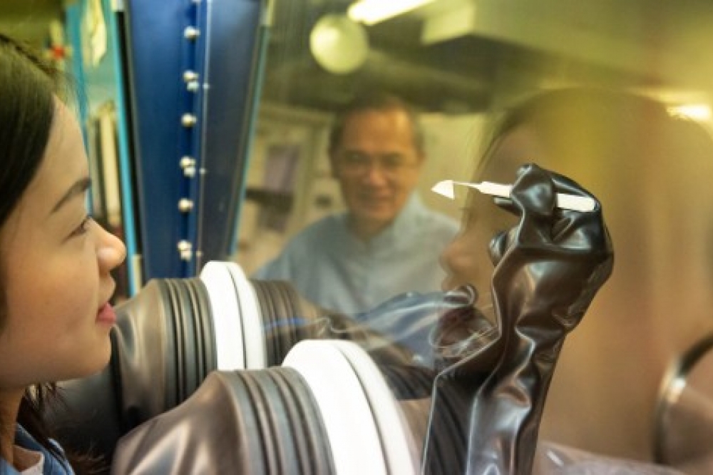
Researchers from the Australian National University (ANU) have reported manufacturing an array of tens of thousands of indium phosphide nanowires and making them glow by incorporating single quantum dot emitters into them. While similar devices have been created before, the team say they have developed a revolutionary manufacturing method that is accurate and fast enough to allow scaling to large-scale on-chip fabrication.
“Our strategy produces single quantum dots in nanowires that have excellent crystal quality, optical performance, and perform extremely efficiently,” said Xiaoying Huang, first author of the paper reporting the breakthrough in the journal ACS Nano, and a member of the ANU Department of Electronic Materials Engineering (EME) and the ARC Centre of Excellence for Transformative Meta Optical Systems (TMOS).
“Our method is also much faster – we grew the array directly in a couple of hours, whereas other research groups using different approaches would take weeks to position the single quantum dots with cavities.”
The single quantum dots are very small, around 13 nm in diameter, which creates better quantum confinement for single-photon sources, that are crucial for quantum information transmission-based devices.
Quantum dots have been used before to make single-photon sources, but a challenge has been to make such small light sources bright enough, in a way that enables deterministic fabrication on a large scale. Encasing them in nanowires addresses this challenge; the internal reflectivity of the nanowire forms an optical cavity around the quantum dot, which increases the intensity of the emitted light.
Initially, physicists tried to manufacture optical cavities by etching – carving the shapes out from a larger piece of indium phosphide that had had quantum dots incorporated in it. However, the synthesis process distributed the quantum dots randomly, which made locating them and then etching cavities around them tricky and time-consuming. Also, the quality was not reliable, as the etching left irregularities on the side walls of the cavities which compromised the emission.
Instead, the EME team decided to turn the approach on its head and grow nanowires from the ground up, using a process called epitaxy, in which atoms are deposited from a vapour. While the team had already perfected the technique for accurately growing arrays of hexagonal indium phosphide nanowires, they faced a challenge in how to embed the single quantum dots inside the nanowires.
Huang explored the droplet epitaxy, a technique in which indium droplets are formed on premanufactured nanowires. At first, she found that multiple droplets would deposit both at the end and along the length of the nanowires. However, by shortening the nanowires, and reducing the droplet deposition time to only 0.25 seconds, she was able to reliably deposit a single droplet onto each nanowire in the 90 micron by 90 micron array.
These droplets are only about 48 nm in diameter and 13 nm high. They are then crystallised into quantum dots (about 13 nm in diameter and 4 nm in height) by adding phosphorus and arsenic to the vapour, converting the droplet to indium arsenide phosphide, a quantum dot that emits light in the near infrared (with a wavelength around 900 nm). Finally, another round of indium phosphide deposition is carried out, which envelops the quantum dot, and increases the nanowire lengths from 3 to 4 microns, and their diameters from 50 to 400 nm.
The finished product can be excited with a red laser to get the quantum dots to emit photons one by one, with this emission enhanced by the encasing nanowire acting as an optical cavity around the quantum dot.
However, not every nanowire performed optimally – while the nanowire cavities can be manufactured reliably and produce consistent cavity wavelength resonance, the quantum dot emission wavelength varies. This is a result of variability in the size and composition of the quantum dots and can cause a mismatch between the quantum dot emission wavelength and the nanowire’s strongest cavity mode, which limits the emission intensity.
Huang believes she can optimise the quantum dot manufacturing process to increase reliability. She is also running simulations to explore different cavity geometries besides nanowires. “While it is challenging from a manufacturing point of view, embedding quantum dots in geometries such as rings or discs could give us a much higher Purcell factor,” she said.


