Aehr receives orders totalling $23 million for test and burn-in products

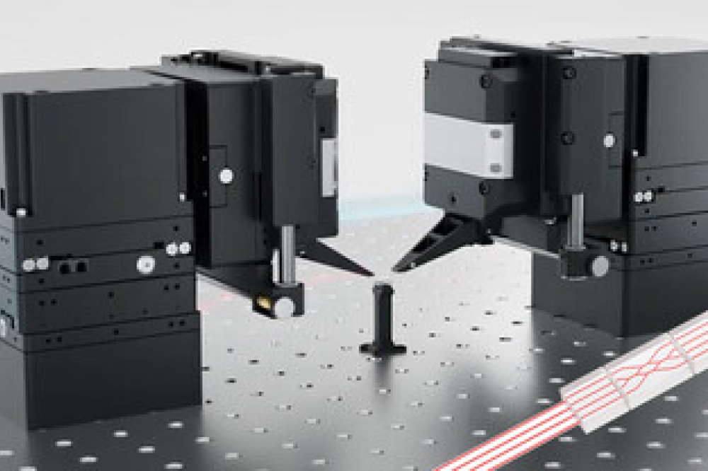
The company says its products are capable of functional test and burn-in of a wide range of integrated circuits, including silicon photonics circuits
Aehr Test Systems, a supplier of semiconductor test and burn-in equipment, has announced it has received new follow-on orders totalling $23 million from existing customers for FOX wafer level test and burn-in products. These products are to be used for production and engineering qualification needs for wafer level burn-in and screening of silicon carbide devices.
The company says the orders include a significant number of FOX WaferPak full wafer Contactors for both current design capacity increases as well as new device designs that are expected to drive additional orders in calendar year 2024 and beyond.
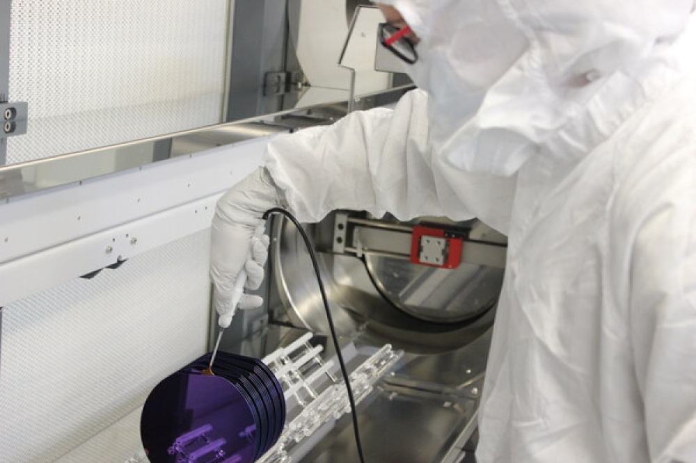
According to Aehr, the FOX WaferPak Contactors are used in conjunction with its FOX-NP and FOX-XP wafer level test and burn-in systems to contact 100% of the die on a wafer up to several thousand devices at a time. The company says these proprietary WaferPak designs are specific to a customer’s application as well as die layout and unique electrical contact pads. Aehr’s FOX systems and WaferPaks are currently being used on wafer sizes ranging from 4 inches to 12 inches and can be configured for a range of device applications.
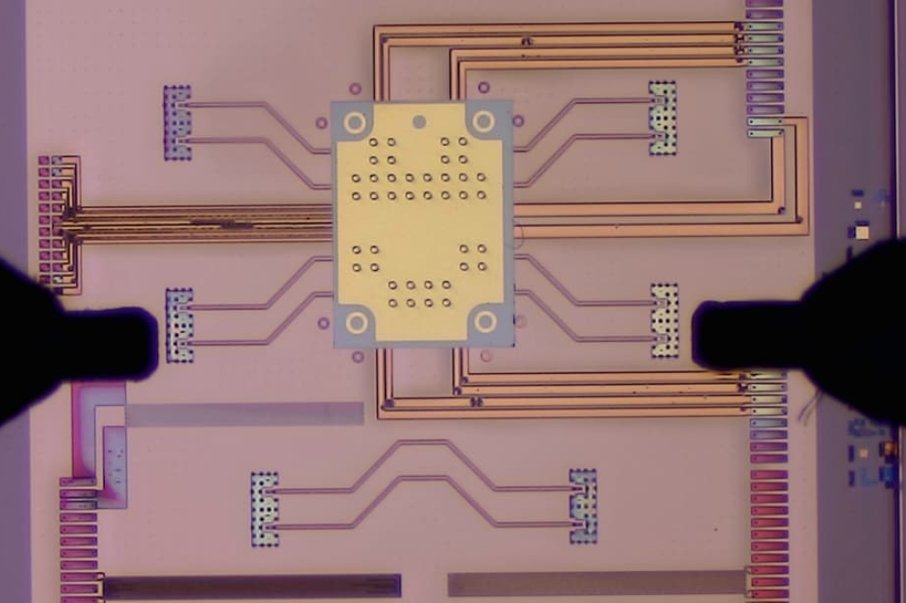
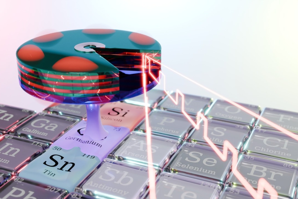
The company says that its FOX-XP and FOX-NP systems and proprietary WaferPaks are capable of functional test and burn-in/cycling of silicon carbide and gallium nitride power semiconductors, silicon photonics integrated circuits as well as other optical devices, 2D and 3D sensors, flash memories, magnetic sensors, microcontrollers, and other leading-edge ICs in either wafer form factor before they are assembled into single or multi-die stacked packages, or in singulated die or module form factor.
“We are excited to help our customers meet their new design and production capacity needs with our industry-leading lead times and capacity for wafer level stress tests, screening, stabilisation, and burn-in,” said Gayn Erickson, president and CEO of Aehr Test Systems. “Our proprietary WaferPak Contactors are unique to each end customer’s device design and grow with the number of device designs and capacity needed for volume production of those devices. As we have stated in the past, we are able to quickly ship a large quantity of WaferPaks with very short lead times with our increased design resources, optimised supply chain, and manufacturing and test processes. We continue to believe our WaferPak business will grow in absolute revenue and also as a percent of the overall revenue for the company. In addition, we have increased our material availability and manufacturing capacity to shorten lead times on our FOX-NP and FOX-XP test and burn-in systems and automated FOX WaferPak Aligners.”


