
Kumamoto plant opening poised to shape Japan’s semiconductor landscape
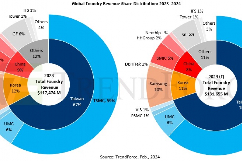
TrendForce’s latest report reveals that in 2023, global foundry revenues hit US$117.47 billion, with TSMC capturing a dominant 60% share.
This figure is expected to climb to around $131.65 billion in 2024, increasing TSMC’s share to 62%. Not only is TSMC leading in revenue, but it has also strategically selected the US, Japan, and Germany as pivotal locations for its advanced and mature factories. Japan is moving at the fastest pace, with some projects even ahead of schedule.
The much-anticipated opening of TSMC’s Kumamoto Plant (JASM) in Japan on the 24th marks TSMC’s debut factory in Japan (Fab-23), signaling a bold step into the future. TrendForce forecasts the plant’s total capacity to hit a robust 40–50K wafers per month (wpm), focusing mainly on 22/28nm processes with a dash of 12/16nm, paving the way for the next phase of the Kumamoto expansion.
Leveraging Its Lead in the Semiconductor Upstream, Japan Eyes a New Semiconductor Era
Japan’s stronghold in the semiconductor industry’s upstream sectors—thanks to leaders like TEL, JSR, SCREEN, SUMCO, and Shin-Etsu—positions it uniquely for the future. TrendForce envisions Japan developing three semiconductor powerhouses in Kyushu, Tohoku, and Hokkaido, with Kyushu taking the lead, especially as the home of TSMC’s Kumamoto plant. Hokkaido’s Rapidus is ambitiously targeting the 2nm process and aiming to spur economic growth. With concerted efforts from industry, government, and academia, Japan is on the brink of creating a comprehensive semiconductor manufacturing ecosystem.
Japan’s semiconductor enterprises are heavily concentrated in Kyushu and Tohoku, with the latter boasting a wealth of talent and a strong focus on semiconductor development at Tohoku University. Highlighting the region’s prominence, companies like ROHM, Renesas, and PSMC are making significant moves, including PSMC’s new 12-inch wafer fab in Sendai. Kyushu’s unparalleled underground water resources, crucial for semiconductor production, have attracted major players like SUMCO and TOK, as well as Sony, ROHM, and Mitsubishi Electric, making it an ideal sport. TSMC’s selection of Kyushu for its expansion was primarily hinged on these water resources.
With the race on for TSMC’s third plant location, other areas in Kyushu like Fukuoka and potentially Osaka in the Kansai region are contenders. Still, in the early planning stages, the project’s future is ripe with possibilities. Initially centered on 6/7nm processes, advancements might lead the third plant to embrace 5nm or 3nm processes as TSMC continues to push the envelope. Beyond this, TSMC’s establishment of a 3DIC research center in Ibaraki and plans for an advanced packaging plant in Japan showcase its commitment to a full-spectrum presence, from front-end manufacturing to back-end packaging and testing, solidifying Japan’s position in the semiconductor sphere.


