Chip uses light to perform calculations needed for AI

By performing many calculations simultaneously, the silicon photonic chip could eliminate the need to store sensitive information, potentially making future computers unhackable, as well as boosting processing speeds and reducing energy consumption
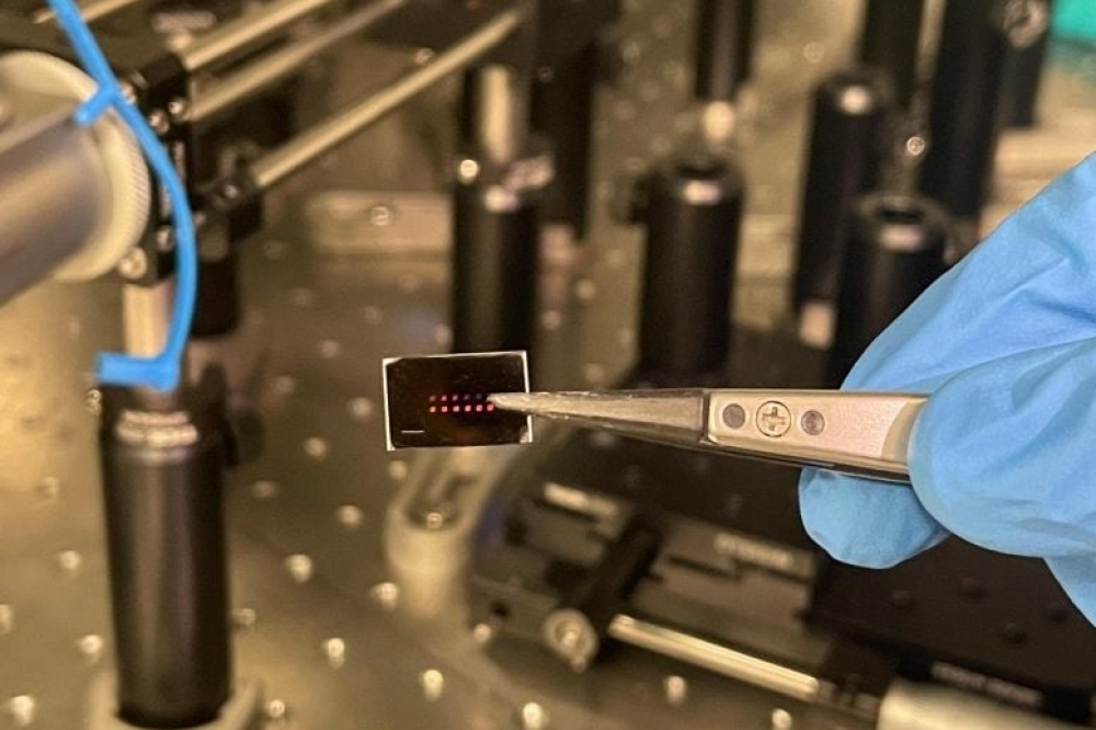
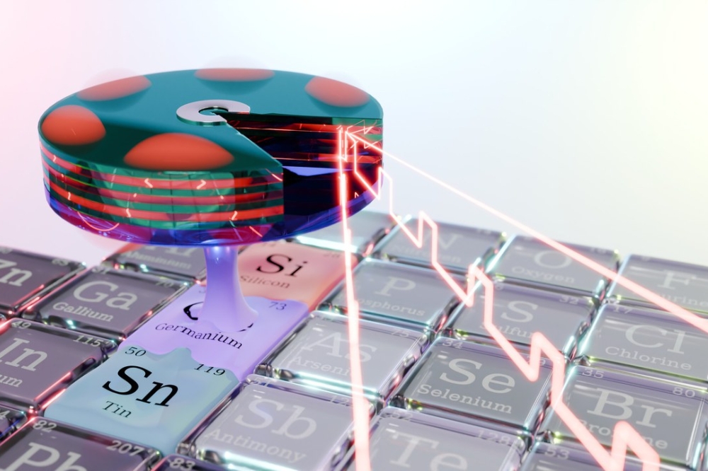
Engineers at the University of Pennsylvania have developed a new chip that uses light waves, rather than electricity, to perform the complex mathematics essential to training AI. The researchers say that this development, reported in a paper in Nature Photonics, could radically accelerate the processing speed of computers while also reducing their energy consumption.
The silicon photonic chip applies the work of Nader Engheta, who is H. Nedwill Ramsey Professor in the School of Engineering, whose expertise includes manipulating materials at the nanoscale to perform mathematical computations using light. In particular, the chip’s design is the first to combine Engheta’s research with the silicon photonic platform, which uses silicon, the cheap, abundant element used to mass-produce computer chips.
The interaction of light waves with matter represents one possible avenue for developing computers that supersede the limitations of today’s chips, which are essentially based on the same principles as chips from the earliest days of the computing revolution in the 1960s.
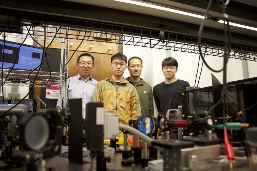
In their new paper, Engheta’s group, together with that of Firooz Aflatouni, associate professor in electrical and systems engineering, describe the development of the new chip. “We decided to join forces,” says Engheta, leveraging Aflatouni’s group’s research on nanoscale silicon devices.
Their goal was to develop a platform for performing what is known as vector-matrix multiplication, a core mathematical operation in the development and function of neural networks, the computer architecture that powers today’s AI tools.
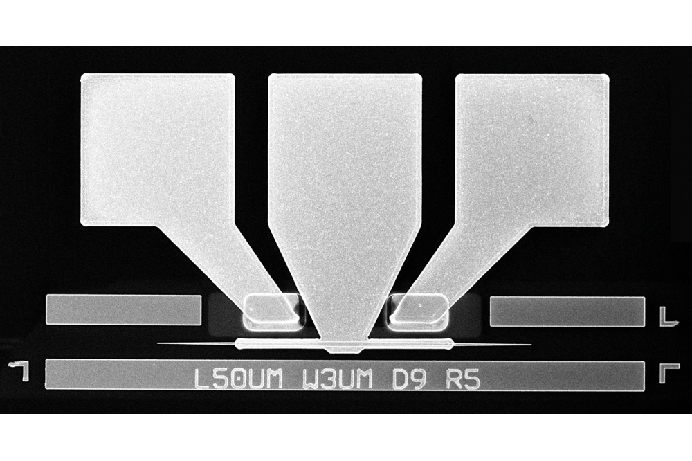
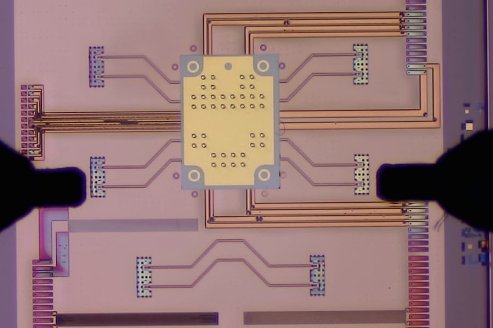
Instead of using a silicon wafer of uniform height, explains Engheta, “you make the silicon thinner, say 150 nm,” but only in specific regions. Those variations in height — without the addition of any other materials — provide a means of controlling the propagation of light through the chip, since the variations in height can be distributed to cause light to scatter in specific patterns, allowing the chip to perform mathematical calculations at the speed of light.
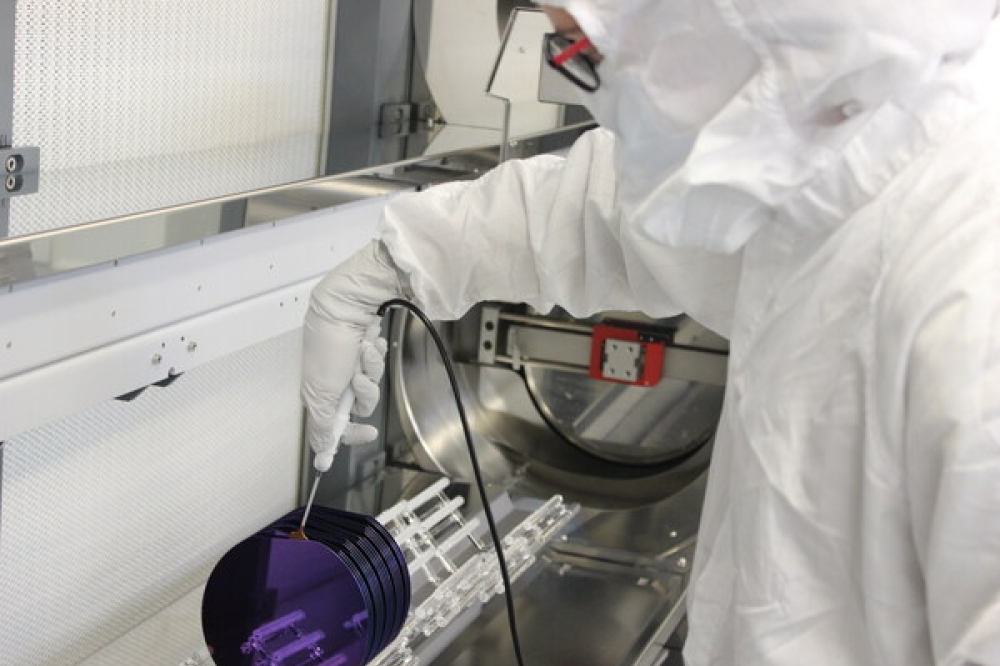
Due to the constraints imposed by the commercial foundry that produced the chips, Aflatouni says, this design is already ready for commercial applications, and could potentially be adapted for use in graphics processing units (GPUs), the demand for which has skyrocketed with the widespread interest in developing new AI systems. “They can adopt the silicon photonics platform as an add-on,” says Aflatouni, “and then you could speed up training and classification.”
In addition to higher speed and lower energy consumption, Engheta and Aflatouni’s chip has privacy advantages; because many computations can happen simultaneously, there will be no need to store sensitive information in a computer’s working memory, rendering a future computer powered by such technology virtually unhackable. “No one can hack into a non-existing memory to access your information,” says Aflatouni.


