
Diamond microchiplet could pave the way for the quantum internet
Tiny diamond waveguides could resolve a key challenge of quantum information transmission, enabling qubits to interact strongly with photons while being undisturbed by environmental noise
In a paper published in Nature Photonics, researchers at MIT and the University of Cambridge report that they have built and tested an exquisitely small device that could allow the quick, efficient flow of quantum information over large distances.
Key to the device is a “microchiplet” made of diamond in which some of the diamond’s carbon atoms are replaced with atoms of tin. The team’s experiments indicate that the device, consisting of waveguides for the light to carry the quantum information, solves a paradox that has stymied the arrival of large, scalable quantum networks.
Quantum information in the form of quantum bits, or qubits, is easily disrupted by environmental noise, like magnetic fields, meaning it’s desirable to have qubits that don’t interact strongly with the environment. However, those qubits do need to strongly interact with light, key to carrying the information over distances.
The MIT and Cambridge researchers allow both by co-integrating two different kinds of qubits that work in tandem to save and transmit information. Further, the team reports high efficiencies in the transfer of that information.
“This is a critical step as it demonstrates the feasibility of integrating electronic and nuclear qubits in a microchiplet,” says Dirk Englund, an associate professor in MIT’s Department of Electrical Engineering and Computer Science (EECS) and leader of the MIT team. “This integration addresses the need to preserve quantum information over long distances while maintaining strong interaction with photons.”
Mete Atatüre, leader of the Cambridge team, adds: “The results are an outcome of a strong collaborative effort between the two research teams over the years. It is great to see the combination of theoretical prediction, device fabrication, and the implementation of novel quantum optical controls all in one work.”
Working at the Quantum Scale
A computer bit can be thought of as anything with two different physical states, such as “on” and “off,” to represent zero and one. In the strange ultra-small world of quantum mechanics, a qubit “has the extra property that instead of being in just one of these two states, it can be in a superposition of the two states. So it can be in both of those states at the same time,” explains coauthor Jesús Arjona Martínez. Multiple qubits that are entangled, or correlated with each other, can share much more information than the bits associated with conventional computing. Hence the potential power of quantum computers.
There are many kinds of qubits, but two common types are based on spin, or the rotation of an electron or a nucleus (left to right, or right to left). The new device involves both electronic and nuclear qubits.
A spinning electron, or electronic qubit, is very good at interacting with the environment, while the spinning nucleus of an atom, or nuclear qubit, is not. “We’ve combined a qubit that is well known for interacting easily with light with a qubit that is well known for being very isolated, and thus preserving information for a long time. By combining these two, we think we can get the best of both worlds,” says Martínez.
“The electron [electronic qubit] whizzing along in the diamond can get stuck at the tin defect,” explains coauthor Isaac Harris. And this electronic qubit can then transfer its information to the spinning tin nucleus, the nuclear qubit.
“The analogy I like to use is the solar system,” Harris adds. “You have the Sun in the middle, that's the tin nucleus, and then you have the Earth going around it, and that's the electron. We can choose to store the information in the direction of the Earth's rotation, that's our electronic qubit. Or we can store the information in the direction of the Sun, which rotates around its own axis. That's the nuclear qubit.”
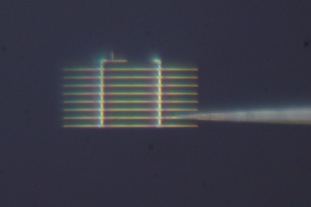
In general, then, light carries information through an optical fibre to the new device, which includes a stack of several tiny diamond waveguides that are each about 1,000 times smaller than a human hair. Several devices, then, could act as the nodes that control the flow of information in the quantum internet.
Although the study only involves experiments with one device, the scientists say that there could eventually be hundreds or even thousands of them on a microchip.
Image credit: Atatüre Laboratory, University of Cambridge


