Luceda Photonics releases PDK in partnership with Luxtelligence
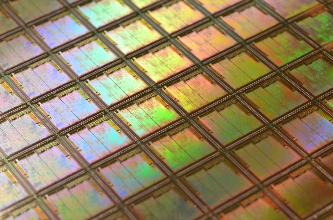
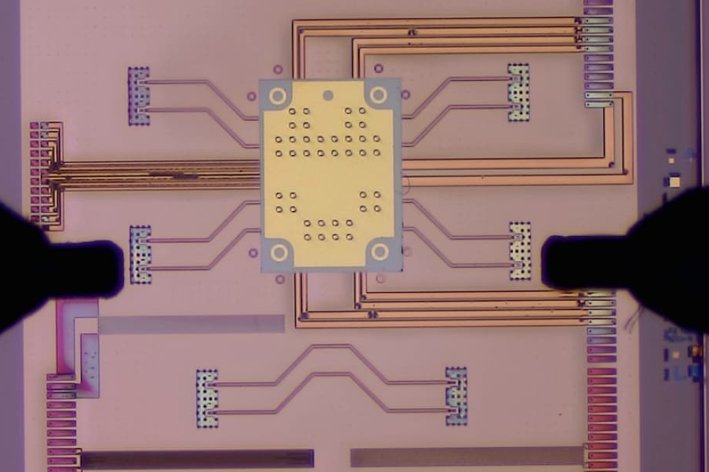
Luceda Photonics and photonic chip manufacturer Luxtelligence have announced the release of the Luceda process design kit (PDK) for Luxtelligence. The companies say this is the start of a collaboration that aims to provide photonic integrated circuit (PIC) designers with access to Luxtelligence’s deep-etch lithium niobate (LiNbO3) technology through the Luceda Photonics design platform.
In recent years, thin film lithium niobate (TFLN) has emerged as a leading platform for next-generation integrated photonics. Leveraging its optical properties, such as large electro-optic coefficient and second-order nonlinearity, wide transparency window (400 nm to 5 µm), and low nonlinear absorption, TFLN has enabled high-performance active integrated photonic devices, unlocking applications in telecommunications, optical frequency combs, and quantum technologies.
This new partnership offers designers and researchers access to Luxtelligence’s patented etching technology for TFLN waveguide fabrication. According to the company, this technology is scalable and ensures extremely accurate dimensional control (40 nm tolerance) with losses lower than 20 dB/m and 3 dB electro-optic bandwidth higher than 40 GHz.
“The release of the Luceda PDK for Luxtelligence marks an important milestone in unlocking new applications based on Luxtelligence’s novel deep-etch TFLN technology and Luceda’s expertise in PIC design enablement,” said Pieter Dumon, CTO at Luceda Photonics. “Luceda is glad to partner with Luxtelligence to make breakthroughs in this advanced technology.”
Mohammad Bereyhi, CEO at Luxtelligence, added: “Our innovative etching technique combines precision and scalability, thus a prototype can be manufactured in volume on our TFLN platform without compromising its performance. In collaboration with Luceda, we are extremely excited to launch a free-access TFLN PDK, which we believe will lower the entry barrier to working with this revolutionary technology.”


