+44 (0)24 7671 8970
More publications     •     Advertise with us     •     Contact us
 
Loading...
Vendor View

AMICRA NOVA Pro from ASMPT

News

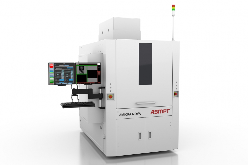
With its new version of the AMICRA NOVA Pro, ASMPT presents one of the most advanced die bonding systems. The platform, which combines high placement accuracy with short cycle times and innovative bonding technologies.

“For speedy data transmissions for precise sensor technology you need equally precise manufacturing technologies,” explains Johann Weinhaendler, General Manager at ASMPT AMICRA in Regensburg, Germany. “To meet the enormous increase in demand in areas like optoelectronics or advanced packaging many electronics manufacturers are currently upgrading their lines. Demand is growing particularly strongly in the silicon photonics sector. For example, you can produce active optical cables for 400/800 Gigabit/sec networks or co-packaged optics with the NOVA Pro.”

Powerful and adaptable

The NOVA Pro places dies in sizes ranging from 0.1 to 25 millimeters with a maximum accuracy of ±1 micron @ 3σ at speeds of up to 1000 units per hour (UPH). At ±3.0 microns @ 3σ it achieves even 3500 UPH. This impressive level of performance is also achieved in flip-chip mode.

The NOVA Pro ensures its trend-setting placement accuracy with its unique dynamic alignment method in combination with laser-based substrate heating technology. And thanks to its Active Bond Force Control, the machine can dose bonding forces with exceptional precision ranging from 10 g to 5000 g. Using an epoxy resin stamp with volumetric dosing, the dies can be affixed with adhesives that get UV-cured in place. The repertoire of precision die fastening methods includes in-situ bonding as well as eutectic die bonding with a bonding tool (up to 350 °C), a ceramic pulse heater (up to 500 °C), or a contactless laser (up to 450 °C). An integrated post-bond inspection ensures maximum quality. With its very generous substrate area of 550 × 600 mm, the NOVA Pro is aimed at the die-bonding market in advanced packaging applications.

Reliable and versatile

“Anyone who opts for the NOVA Pro benefits from the many years of experience of the market leader, who is fully committed to the goal of zero DPMO,” says Johann Weinhaendler. “The high reserves in terms of precision and performance as well as the flexible fixation and bonding options make this machine a future-proof investment.”

Samco Inc announces sale of etching systems to III-V Lab
European Innovation Council funds QuiX Quantum
Intel and Source Photonics partner on 800G transceivers
LioniX secures €1.5 million in bridge financing
A technique for 3D nanostructuring inside silicon
Senergetics wins Gerard and Anton Award
Scantinel announces new CMOS-based LiDAR chip
Project to miniaturise spectrograph wins €3.4 million
EU invests €325 million in Europe's semiconductor ecosystem
Fraunhofer IPMS developing near-infrared silicon-based photodiodes
PhotonDelta opens US office in Silicon Valley
EU funds integrated photonics for space navigation
Maryland Department of Commerce funds PIC testing and packaging facility
Lightmatter appoints Simona Jankowski as chief financial officer
scia Systems to showcase ion beam processing advances at SEMICON West
Quantifi Photonics announces Iannick Monfils as new CEO
Nokia and TTI achieve 800G on long-haul commercial network
Nokia to acquire Infinera for $2.3 billion
Advancing AI with programmable silicon photonics
Quantum PICs: Empowering designers with accurate simulations
Enabling efficient light emission and detection
Harnessing InP for applications beyond optical communications
POET wins “Best Optical AI Solution” in AI Breakthrough Awards
Intel reveals fully integrated optical I/O chiplet
People, planet, profits: a sustainable way forward for all
A bright future for the global PIC market
Atom-thin silicon-germanium sheets for integrated photonics
BAE Systems and GlobalFoundries partner on semiconductors
Wave Photonics raises £4.5 million in seed funding
Aeva to supply LiDAR for AutomatedTrain project in Germany
Black Semiconductor raises €254.4 million for graphene chips
Pooya Tadayon joins Ayar Labs

×
Search the news archive

To close this popup you can press escape or click the close icon.
Logo
×
  • 1st January 1970
  • 1st January 1970
  • 1st January 1970
  • 1st January 1970
  • 1st January 1970
  • 1st January 1970
  • 1st January 1970
  • 1st January 1970
  • View all news 22645 more articles
Logo
×
Register - Step 1

You may choose to subscribe to the PIC Magazine, the PIC Newsletter, or both. You may also request additional information if required, before submitting your application.


Please subscribe me to:


You chose the industry type of "Other"

Please enter the industry that you work in: