
Fraunhofer IPMS to present customised tech at SPIE Photonics West
The Fraunhofer Institute for Photonic Microsystems IPMS has revealed some of the technology it will be presenting at the SPIE Photonics West conference and exhibition in San Francisco from 27 January to 1 February 2024. The institute will showcase developments and advances in areas such as micro-optics, MEMS-based light modulators and biophotonics.
Label-free detection with photonic biosensors
Label-free detection methods – methods without additional reagents for molecular characterisation – have a high application potential. They offer simpler medical diagnostic tools that can be used outside the laboratory, making them accessible to non-specialist users. Fraunhofer IPMS develops photonic label-free biosensors based on integrated photonic components fabricated in silicon nitride technology, such as microring resonators and Mach-Zehnder interferometers. They are used for the selective detection of biomarkers or microbial substances and offer a suitable detection method for the early detection of diseases, for example.
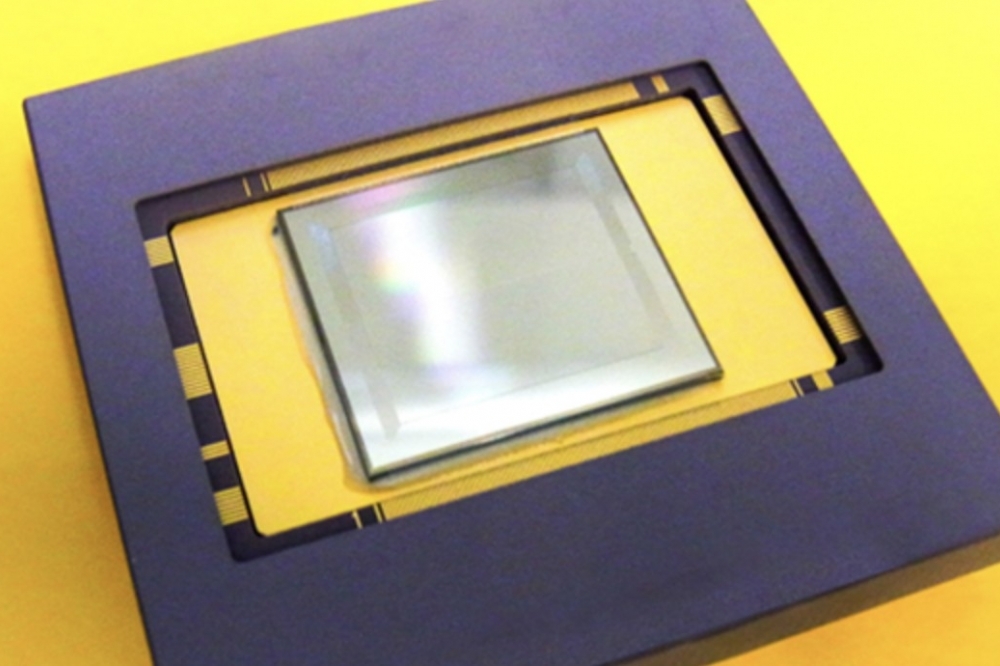
Photonic microsystems for high-resolution lighting control
Fraunhofer IPMS develops spatial light modulators with up to several million mirrors on a semiconductor chip. So-called piston micromirror arrays enable high frame rates and high-precision wavefront modulation. A new field of application is the generation of computer-generated holograms in applications such as augmented, virtual and mixed reality.
The micromirror arrays (MMA) developed at the institute are characterised by precise analogue control of the deflection of each individual pixel and a wide wavelength range. Other potential applications include high-resolution DUV microlithography, adaptive optics and wavefront control. The latest characterisation and simulation results will be presented in a talk at SPIE Photonics West, while various examples of real micromirror arrays and enlarged functional models will be on show at the exhibition stand.
Custom MEMS scanner design and qualified production
Fraunhofer IPMS has extensive expertise in the development and production of MEMS scanners based on monocrystalline silicon. These components are characterised by large scanning angles, high scanning frequencies, on-chip position sensors and excellent long-term stability.
At the trade fair, the research institute will present a novel electrostatically driven vector scanner that can be used for rapid beam positioning of a compact medical therapy laser. The laser was developed for the treatment of retinal diseases, and features high precision and speed of the vectorial beam positioning combined with high energy efficiency and suitability for high laser power.
In addition, this approach allows the fabrication with Fraunhofer IPMS' own AME75 technology, so that all combinations of vectorial (quasi-static) positioning and resonant scanner oscillation 1D, 2D can now be realised with one fabrication technology. This significantly expands the design space for Fraunhofer IPMS MEMS scanners.


