
Chipscale laser emits precise light in both NIR and visible
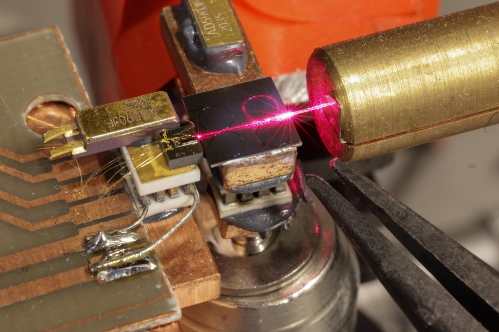
Image credit: 2023 EPFL/Alain Herzog - CC-BY-SA 4.0
The team at EPFL’s Photonic Systems Laboratory (PHOSL) has reportedly developed a chipscale laser source that enhances the performance of semiconductor lasers while enabling the generation of shorter wavelengths. Led by Professor Camille Brès and postdoctoral researcher Marco Clementi from EPFL’s School of Engineering, the researchers say this represents a significant advance in the field of photonics, with implications for telecommunications, metrology, and other high-precision applications.
The study, published in the journal Light: Science & Applications, describes how the PHOSL researchers, in collaboration with the Laboratory of Photonics and Quantum Measurements, integrated semiconductor lasers with silicon nitride photonic circuits containing microresonators. The team says this integration results in a hybrid device capable of emitting highly uniform and precise light in both near-infrared and visible ranges, filling a technological gap that has long been a challenge for the industry.
“Semiconductor lasers are ubiquitous in modern technology, found in everything from smartphones to fibre optic communications,” explains Professor Brès. “However, their potential has been limited by a lack of coherence and the inability to generate visible light efficiently. Our work not only improves the coherence of these lasers but also shifts their output towards the visible spectrum, opening up new avenues for their use.”
Coherence, in this context, refers to the uniformity of the phases of the light waves emitted by the laser. High coherence means the light waves are synchronised, leading to a beam with a very precise colour or frequency. This property is crucial for applications where precision and stability of the laser beam are paramount, such as timekeeping and precision sensing.
Increased accuracy and improved functionality
The team's approach involves coupling commercially available semiconductor lasers with a silicon nitride chip. This tiny chip is created with industry-standard, cost-efficient CMOS technology. Thanks to the material’s low-loss properties, the researchers say that little to no light is absorbed or escapes. The light from the semiconductor laser flows through microscopic waveguides into extremely small cavities, where the beam is trapped. These cavities, called micro-ring resonators, are intricately designed to resonate at specific frequencies, selectively amplifying the desired wavelengths while attenuating others, thereby enhancing coherence in the emitted light.
The other significant achievement is the hybrid system’s ability to double the frequency of the light coming from the commercial semiconductor laser— enabling a shift from the near-infrared spectrum to the visible light spectrum. While the near infrared spectrum is exploited for telecommunications, higher frequencies are essential for building smaller, more efficient devices where shorter wavelengths are needed, such as in atomic clocks and medical devices.
These shorter wavelengths are achieved when the trapped light in the cavity undergoes a process called all-optical poling, which induces what is known as second-order nonlinearity in the silicon nitride. This means that the light’s interaction with the material causes a significant shift in the light's behaviour that is not directly proportional to its frequency. Silicon nitride does not normally induce this specific second order nonlinear effect, and the team deliberately engineered it to do so. The system takes advantage of the light’s capacity, when resonating within the cavity, to produce an electromagnetic wave that provokes the nonlinear properties in the material.
An enabling technology for future applications
Marco Clementi, who played a key role in the project, says: “We are not just improving existing technology but also pushing the boundaries of what's possible with semiconductor lasers. By bridging the gap between telecom and visible wavelengths, we're opening the door to new applications in fields like biomedical imaging and precision timekeeping.”
One of the most promising applications of this technology is in metrology, particularly in the development of compact atomic clocks. “This significant advancement lays the groundwork for future technologies, some of which are yet to be conceived,” adds Clementi.


