
Spirox and Southport launch non-destructive wafer defect inspection system
Spirox Corporation, a provider of semiconductor testing solutions, and its subsidiary, Southport Corporation, have launched a new defect inspection system for silicon carbide (SiC) wafers. The companies say their JadeSiC-NK product is an industry-first non-destructive system that can improve yields and reduce costs.
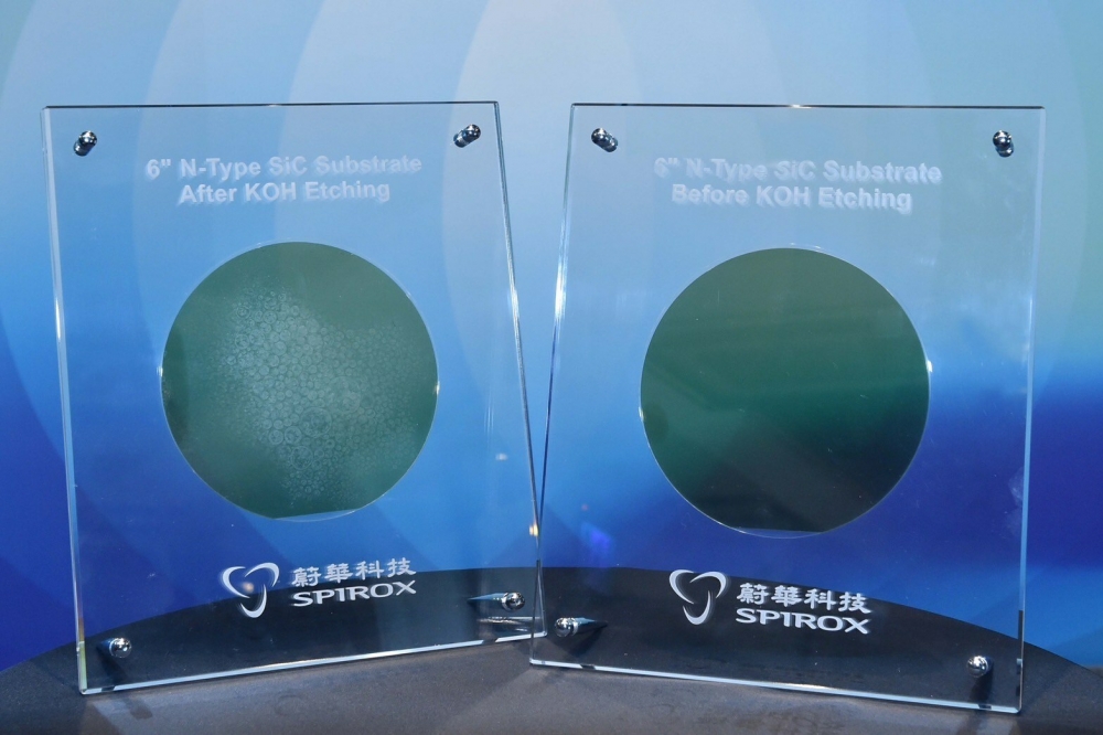
The quality of substrate materials determines the reliability and performance of SiC chips. However, the number of defects and distributions of the substrate crystal can only be inspected by sampling with mathematic interpolation when using the current destructive potassium hydroxide (KOH) etching method. If SiC substrate manufacturers can implement non-destructive inspection of materials in the manufacturing process, it will not only reduce the usage of harmful chemical solutions associated with KOH etching but also allow for the early detection of defects.
JadeSiC-NK employs non-linear optical technology for whole-wafer scanning of SiC substrates to identify killer defects. Spirox and Southport say that the system can be a substitute for the high-cost, destructive KOH etching method, leading to increased production yields and process improvement. The companies calculate that, based on the need to etch two substrates for each SiC ingot in the KOH process, JadeSiC-NK can save approximately $7.68 million in annual costs incurred due to etching losses for a substrate manufacturer with 100 crystal growth furnaces.
CEO of Spirox, Paul Yang, said: “Spirox has been continuously enlarging its investment to develop solutions to fulfil customer needs. With Southport, Spirox expands our product portfolio from semiconductor testing equipment to optical inspection. The initial focus is on the highly promising defect inspection of compound semiconductor materials. Besides applying non-linear optical technology in the newly launched JadeSiC-NK, Spirox plans to accelerate the commercialisation of advanced optical inspection technologies in areas such as MicroLED, metamaterial, silicon photonics, etc., in the future.”
Ken Tai, chairman of Taiwan Photonics Industry & Technology Development Association, added: “It's a great pleasure to see two Taiwanese companies creating synergy through a mutually beneficial collaboration, generating tremendous value for the industry. JadeSiC-NK represents a groundbreaking technological breakthrough. It's not only a revolutionary product for the booming global compound semiconductor industry, capable of significantly reducing costs and increasing production capacity, but also showcases Taiwan's technological leadership with Spirox and Southport as representatives.”


