
A toolbox for photonic quantum computing
A mature integrated photonics platform is essential for building scalable photonic quantum devices. Quantum pioneers can access it by partnering with imec as a technology provider with a flexible CMOS fab.
By Amin Abbasi, Senior Business Development Manager, imec
Will we have a quantum computer one day? There has been a tremendous amount of progress over the last few years – with breakthroughs that were destined to make media headlines. Nevertheless, you’d be hard-pressed to find a quantum expert who’s prepared to give youa 100 percent guarantee that practical quantum computing is already on the horizon.
The main hurdle is scalability. Although physical qubits are essential building blocks of future quantum computers, obtaining them is, more or less, the ‘easy’ part. The more significant challenge is making the necessary connections between thousands or even millions of them. That’s why, in the debate on the preferred method for producing physical qubits, scalability is quickly becoming a decisive argument. It also goes a long way towards explaining why photonics-based quantum computing – a relative newcomer compared with well-established contenders such as superconducting- and semiconductor-based quantum computing – has been attracting much attention lately.
In this article, we look at what makes photonics such a promising match for quantum computing, and we’ll enumerate the existing challenges and how they can be addressed. We also want to highlight imec’s role, not only as an application company for quantum computing using integrated photonics, but also as a technology provider to its valued customers.

Most methods for acquiring qubits require cryogenic cooling, hampering scalability. Source: Getty Images
Harnessing the unshakeable power of photons
Qubits are the primary carriers of information in a quantum computer. In contrast with bits in classical computing, which are constrained to ones or zeros, qubits can be in multiple states simultaneously (ones, zeros and combinations of ones and zeros). String them together, and they contain amounts of information that scale exponentially to astronomical proportions.
Despite this superpower, qubits in their physical form are incredibly delicate. Their decoherence time is very short, meaning that, when you put them in a quantum state, they quickly lose it again. This makes it difficult to do computation, and it
can only be counteracted by cooling them to cryogenic temperatures, preventing interactions with their environment. That’s why the quantum computer prototypes we know so well are surrounded by a roomful of cooling infrastructure, and it partly explains why the scaling challenge is so huge.
There are, however, certain kinds of qubits, such as physical qubits based on near-infrared optical photons, that are less dependent on cryogenic cooling to tens of millikelvins. This is because the energy of optical photons (~ 1 eV) is orders of magnitude larger than the thermal noise at room temperature (~23 meV).
Once you put these photons in a quantum state, they maintain it as long as they can travel freely, potentially making a room-temperature quantum computer more than just a fantasy. But before we can make it a reality, there are plenty of challenges left to solve.

Overview of imec’s silicon photonics platform. Source: imec
Every photon counts, so count every photon
What is the basic layout of a photonics-based quantum computer? An ideal light source produces single photons – a considerable challenge in itself. Then, linear optical elements such as beam splitters and phase shifters implement qubits and logic gates. Finally, photodetectors read out the final states by measuring the arrival of single photons.
Such a system has been set up in free space for lab demonstration purposes, producing a handful of qubits. But setups like this have zero scaling potential. A true photonics-based quantum computer with thousands or even millions of qubits can only be achieved by bringing all components onto a highly integrated on-chip platform.
The good news is that quantum computing development can plug into a rapidly growing silicon photonics ecosystem that leverages the mature semiconductor manufacturing infrastructure to make photonic structures – from waveguides to phase shifters – on silicon chips. This considerably lowers the barrier for pioneering companies in the quantum photonics domain, as they don’t need to start from a blank slate but can at least partly use existing modules.
Still, photonics for quantum is a different game than photonics for existing applications like telecommunications. By far the biggest challenge when designing photonic circuits for quantum is controlling loss; in the quantum space, every single photon is a vessel for information that should not be lost. Imagine such a photon traveling through centimetres or even metres of waveguide with a propagation loss of 2 or 3 dB per centimetre. The chances are that it will not arrive at the end and will not get measured.
On top of this propagation loss, coupling loss is an equally pressing issue. Making a quantum computer with thousands or millions of qubits will require dozens of chips to be connected. The signal integrity at these interconnections has to be guaranteed for photonic quantum computing to stand a chance.
Such ultra-low-loss structures are not feasible using silicon photonics alone. Other materials, such as silicon nitride (SiN), will be needed – preferably while retaining tight integration with a silicon platform that is still required for other components, such as the driving electronics.

200 mm SiN wafer processed at imec. Source: imec
Bridging the gap between lab and fab
As a leading semiconductor R&D hub, imec took an early interest in quantum computing. We’re conducting research into promising options for the development of physical qubits, such as spin qubits and superconducting qubits, as well as cryogenic 3D integration. Our strategy towards photonic quantum computing, however, is somewhat different.
While we are pursuing some fundamental research in the photonic quantum domain – such as 2D-based single photon emitters (with Ghent University and MIT) – we mainly aim to advance the field by sharing our infrastructure and expertise with our partners from the industry. The reason for this approach is that we see many companies, especially start-ups and scale-ups, struggling to bridge the divide between their idea or concept – even a first lab-developed prototype – and commercialisation.
We can consider that divide as stemming from the difference between an academic lab and a commercial foundry. University labs are where most start-ups originate. They offer the flexibility to explore different concepts and produce creative solutions. However, they lack advanced capabilities – including industry-grade tools – that allow the development of a manufacturable prototype, which is needed to convince investors once you want to scale up.
However, when companies turn to foundries to manufacture such a prototype or do a low-volume run, they often come up against a brick wall. Very few foundries have the flexibility to take on such small projects, being booked to the brim with profitable high-volume runs.
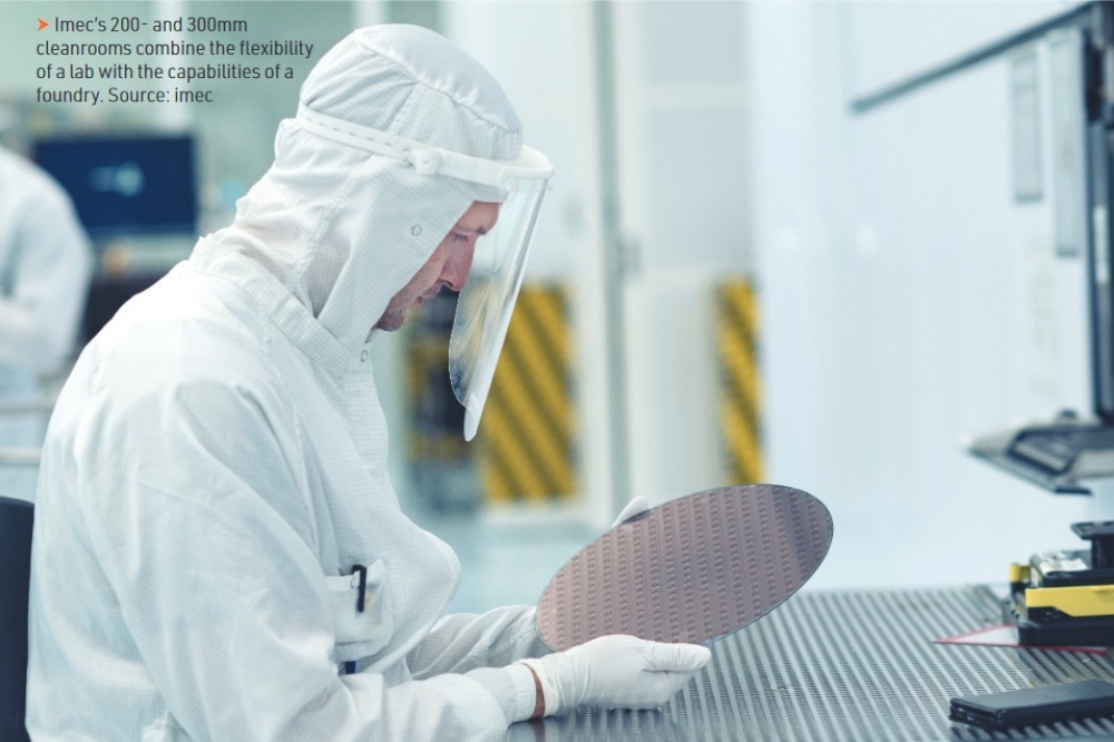
As a semiconductor R&D centre with strong ties to the industry, imec can bridge that gap by combining the flexibility of a lab with the capabilities of a foundry. In our 200 mm and 300 mm cleanrooms, partners can develop a process or a prototype that’s guaranteed to be compatible with the standard industry tools. We can even handle low-volume runs of their product – up to a few hundred wafers per year – or transfer the technology to a customer-preferred CMOS foundry for high-volume production.
Considering the importance of scalability when it comes to quantum, that’s a significant advantage for aspiring companies. One such company is Xanadu, which partnered with imec to develop photonic chips for fault-tolerant quantum computing.
In the words of Zachary Vernon, head of Xanadu’s hardware team, “one of the most critical challenges in building a photonic quantum computer is finding the right fabrication partner that can simultaneously deliver innovative process development and volume production of high-performing photonic chips. Imec is one of the few semiconductor R&D centres that does advanced technology R&D on advanced 200 mm and 300 mm lines, as well as volume manufacturing on their 200 mm line. The seamless transfer offered by imec of new processes to production is especially critical for the rapid scaling of our technology.”

Artist’s impression of an external-cavity diode laser (ECDL) array.
Inset: scanning electron microscope (SEM) picture of a bonded DFB laser.
Source: imec
Photonic quantum computing toolbox
Let’s now look at the toolbox that imec offers partners that want to push the boundaries of photonic quantum computing. The ultimate goal is clear: combine all quantum computing functions (sources, circuits and detectors) on one photonic integrated circuit, overcoming specific challenges, such as the need for ultra-low loss.
To reach this goal, we leverage our mature and versatile integrated photonics platform. We perform customisations and add new modules to meet our partners’ needs. Imec has two integrated photonics platforms: silicon photonics, based on silicon-on-insulator (SOI), and silicon nitride photonics, based on thin-film SiN. Our silicon platform contains many high-speed active and passive modules. It’s mainly geared towards datacom and telecom applications, but it also includes basic building blocks for quantum, such as a PIC-based quantum engine, high Q-ring resonators, and edge couplers. Meanwhile, our silicon nitride platform is ideal for non-communication applications such as sensing, biophotonics, and metrology. But silicon nitride also holds critical benefits for the development of quantum applications. In particular, its extremely low propagation loss (0.2 dB/cm down to a couple of dB/m) and its high tolerance for thermal variations of the environment make it a good candidate for quantum.
Finally, multiple other materials with wide index variations can be integrated, such as titanium oxide, niobium oxide, aluminium oxide, and silicon oxide. Different substrates are also possible, such as doped glass and quartz.
This portfolio allows us to build solutions tailored to our partners’ needs. New modules are constantly being developed, such as novel electro-optical modular integration, wafer-to-wafer bonding, and wafer-scale laser integration through an RSO/DFB flip-chip process.
Conclusion: a shortcut from idea to manufacturable quantum device
In the race towards a practical quantum computer, photonic quantum computing is a strong contender. Its presumed ability to function at room temperature makes the crucial issue of scaling somewhat easier. However, the challenge remains formidable, with the need to achieve ultra-low propagation loss and coupling loss as one of the main hurdles to overcome.
The good news is that years of experience with integrated photonics have resulted in mature platforms that support a lot of the building blocks needed for photonic quantum computing. What’s more, these platforms leverage the existing mass manufacturing tools of the semiconductor industry, which ensures an effortless route to further scaling once the initial R&D obstacles are solved.
Due to its unique position in the semiconductor ecosystem, between academia and industry, imec can offer photonic quantum computing companies a flexible environment to do initial R&D and the opportunity to develop their solutions using industry-grade tools. That allows them to take a shortcut from concept to manufacturable device, inching us closer to a technology that promises to crack some of humankind’s biggest problems.
Main image Imec’s 200 and 300mm cleanrooms combine the flexibility of a lab with the capabilities of a foundry. Source: imec


