ECOC 2023 explores the future of photonics
From artificial intelligence and machine learning to quantum 2.0, focused sessions discussed how PICs can be scaled and evolved to support exciting applications.
By Laura Hiscott, Editor, PIC Magazine
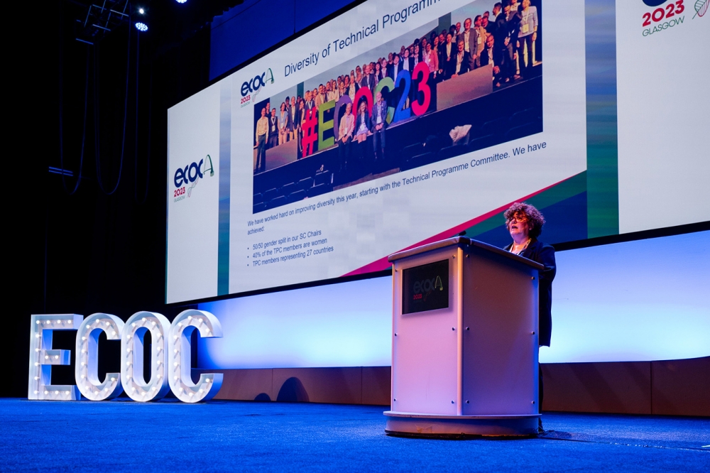
Photonic integrated circuits were very much on the agenda at the 49th European Conference on Optical Communication (ECOC), which was held in Glasgow from 1-5 October.
On the first morning, a workshop on “Scaling Routes in Silicon Photonics” reflected on the growth that the sector has experienced in recent years, and explored potential strategies for boosting current volumes even further to establish a sustainable ecosystem. Thomas Liljeberg from Intel opened the session with a talk on heterogeneous integration, reporting on Intel’s work integrating InP lasers onto silicon platforms.
He emphasized how this can overcome the input/output costs, while taking advantage of the reliability of CMOS manufacturing. Focusing on the data-hungry application of AI, Liljeberg outlined how integrating multiple channels onto a chip can offer higher bandwidth, and how, for reliable fabrication processes, cost per channel drops as the channel number increases.
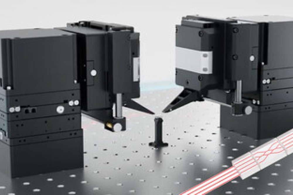
In the same workshop, Kamil Gradkowski from Tyndall National Institute addressed the need for faster, cheaper packaging processes, highlighting that, together, assembly, packaging, and alignment can account for up to 80 percent of a device’s total cost. To tackle this, he presented recent work on pluggable couplers that are designed with microlenses that can collimate the light between the chip and the fibre, expanding alignment tolerances.
Image credit: Sarah Sennett
These pluggable couplers offer an opportunity for standardisation, since they should be compatible with any photonic chip, provided it has the correct microlenses attached to it. Gradkowski also described collaborative work with the packaging manufacturer ficonTEC, demonstrating that the process of attaching microlenses to a chip can be automated with the company’s machines, offering another advantage for scalability.
While PICs are useful in optical communications in general, one session at ECOC focused in on how they could be particularly useful for quantum technologies. Introducing the symposium, “PICs for Quantum,” John Marsh from the University of Glasgow spoke about the proposal of a National Institute for Quantum Integration (NiQi), a potential UK-wide programme to accelerate the commercialisation of quantum technology. A trial of the concept – the NiQi Pilot Accelerator – is currently underway in the form of a two-year Glasgow-based initiative that is supported by the Department of Science, Innovation & Technology, Innovate UK, and Glasgow City Region.
The session went on to cover a wide range of quantum applications of photonics. Andrew McKee from Sivers, a designer and manufacturer of lasers, spoke about the company’s collaborative work to apply their technology to atomic clocks, quantum magnetometers, and LiDAR systems. Meanwhile, Jon Heffernan from the University of Sheffield presented developments in the fabrication of quantum dots as single-photon sources for quantum photonic circuits, and Jonathan Silver from NPL discussed how PICs could be used to miniaturise atomic clocks.
Describing why PICs are well suited to quantum applications, Peter Smith from the University of Southampton cited the value of being able to do wavelength conversion and generate entangled pairs of photons. He also highlighted that integration is key, given that quantum technology cannot tolerate any loss of photons, unlike telecom, which can compensate for insertion loss by amplifying the signal. Smith also spoke about Covesion, a company he co-founded, which makes periodically poled lithium niobate (PPLN). He described how PPLN waveguides can perform efficient wavelength conversion and thus act as a narrow linewidth source of wavelengths corresponding to specific quantum transitions, such as those of rubidium atoms.
Image credit: Ian Arthur Photography
An interesting message from Smith’s talk was that the community might benefit from being open-minded about the route to fully commercialised quantum applications and how long it might take. Contrasting photos of the Colossus computer, which was built in the 1940s, and the Apple M1 chip, released in 2020, Smith pointed out that it took over 70 years to get from the former to the latter, and that numerous technologies had to be developed to facilitate that transition. “In this quantum space there’s a danger of thinking ‘we need a mass-market solution now,’” he said, “and that might not be true because these two pictures are 76 years apart.”
We don’t know how long it will take to realise the promises of the quantum revolution, or all the intermediate technologies we might need to develop along the way, but fundamental research in this space is essential. It will be fascinating to see what progress has been made in a year’s time, at ECOC 2024.


