State-of-the-art electronic photonic design automation

Through partnerships with foundries and electronic design automation (EDA) tool providers, Ansys has created a comprehensive Electronic Photonic Design Automation (EPDA) solution, featuring the co-design and co-simulation of EICs and PICs.
BY RAHA VAFAEI, ZEQIN LU, AHSAN ALAM, PARYA SAMADIAN, FEDERICO DUQUE GOMEZ AT ANSYS
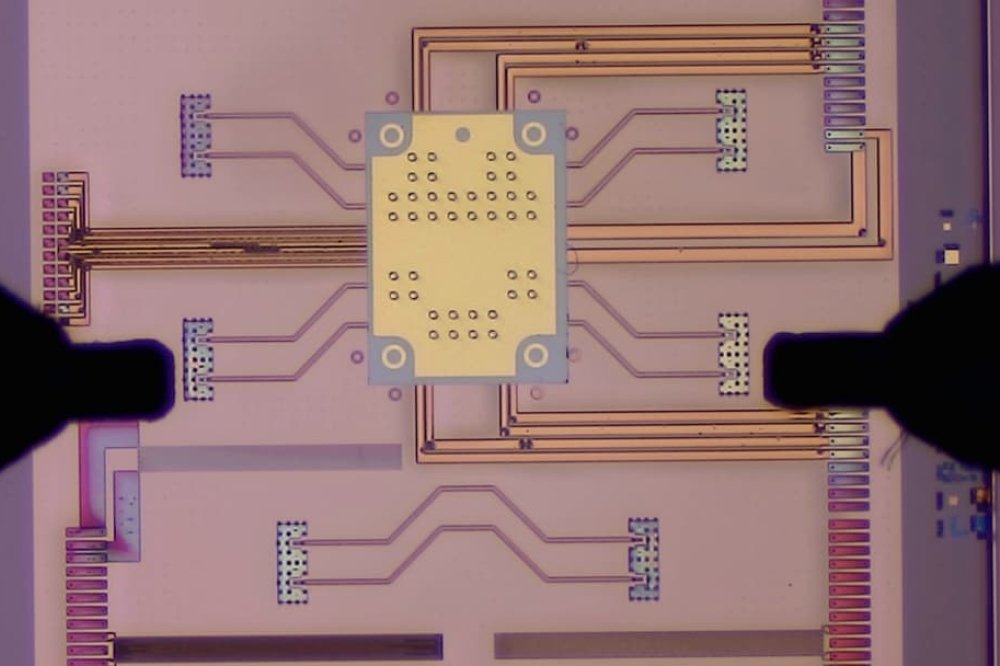
In recent years, photonic integrated circuits have been on a trajectory of ever-increasing design complexity, driven primarily by the massive growth in data, and the growing demand for high performance, low power consumption, and low cost. To meet these demands, the PIC industry has evolved to emulate the world of electronics. In electronics, foundries can yield hundreds of chips on a single wafer, each one meticulously designed by engineers and incorporating billions of transistors, with each transistor about 1000 times smaller than what the human eye can perceive.
The electronic industry owes this incredible success largely to the maturity of the CMOS manufacturing facilities and the electronic design automation (EDA) tools and workflows. Similarly, to meet the growing demands for photonic solutions, the industry has responded with an orchestrated effort between foundries and design tool providers to create an electronic photonic design automation (EPDA) ecosystem. In collaboration with foundries and other EDA providers, Ansys has developed EPDA workflows built on best-in-class tools that meet photonic design requirements while embracing flexibility for designers to run on their preferred platforms. Figure 1 shows an overview of our multiplatform EPDA solution which enables designs from a component to a working chip.
Figure 1: In collaboration with third-party EDA and Layout tool
providers, Ansys Lumerical enables scalable designs, from concept to a
working chip.
Multiplatform photonic system design
Photonic integrated circuits are often controlled or driven by electronic integrated circuits (EICs). Ideally, EICs and PICs should be co-designed in a single schematic and be co-simulated to capture the tight interaction between the optical and electrical domains, such as photonic components’ loading effects on the EICs and the electrical feedback loops between the two domains. This allows designers to analyse and optimise the overall performance.
When it comes to simulating purely a photonic circuit, the simulation can be done entirely in Lumerical INTERCONNECT which provides a schematic design environment with a circuit simulator purpose-built for simulating complex photonic integrated circuits. To design a complex photonic chip with EIC controls, however, it is important to model the full electro-optical circuit. To this end, Ansys Lumerical and Cadence have partnered over the years to provide the industry’s first and most mature EPDA environment. The integration between Cadence Virtuoso and Lumerical INTERCONNECT means users can take advantage of these two engines for the photonic and electronic parts of their system respectively. In this seamless integration, the Virtuoso schematic design environment is used for complete schematic capture of the system, including the photonic and electronic sub circuitries. Virtuoso ADE can co-simulate by simultaneously running Spectre and INTERCONNECT engines in the background and exchanging data to solve the full system.
For simulating full electro-optical circuits, Ansys Lumerical also provides advanced photonic Verilog-A models: analogue behavioural models that can be solved by SPICE solvers and are commonly used in the electronics world. Photonic Verilog-A models describe the behaviour of photonic elements using the standard Verilog-A language, leveraging the maturity of the corresponding electrical methods. Hence these models are also ideal for full electro-optical system simulation in EDA platforms like Cadence Spectre. Using advanced photonic Verilog-A models from Ansys, Spectre can solve both electrical and optical parts of the circuit.
Figure 2: The left-hand side of the figure shows the complete schematic
capture in Cadence Virtuoso including the photonic transceiver, CMOS
drivers, and TIAs. The right side shows the ring-based, 4-channel DWDM
transceiver circuit.
All the above platform options for modelling PICs have been developed to meet the unique requirements of optical signals, taking into consideration amplitude, phase, multi-wavelength, bidirectional and multimodal behaviour. It is important to note that all these platforms deliver consistent results as the models have been thoroughly verified for the physics and workflows they support.
We will now consider the co-design and co-simulation of a 4-channel, dense-wavelength-division-multiplexing (DWDM) silicon photonic transceiver and its electrical drivers and receivers as shown in Figure 2. The design consists of continuous-wave (CW) laser sources, a photonic transmitter (Tx) chip, a photonic receiver (Rx) chip, high-speed CMOS drivers, and transimpedance amplifiers (TIAs). We leverage our Cadence schematic-driven flow to design the photonic circuits and the electronic circuits and compare the results of the co-simulation using INTERCONNECT models with the results of electro-optical simulations using the Verilog-A models. Figure 2 shows the complete schematic capture in Virtuoso including the photonic transceiver, CMOS drivers, and TIAs. Comparing the electronic-photonic co-simulation using INTERCONNECT models versus running Verilog-A models, we can see consistent results in key measures of performance, such as rise/fall time and eye-opening, as shown in Figure 3.
Multiplatform photonic PDK generation
The precision of a circuit’s simulation results relies on the fidelity of the models employed in its building blocks. Accurate models are established through rigorous component-level simulations, measurements derived from device characterization, or a combination of both approaches. The complexity of multiphysics effects within these devices necessitates models that can capture their intricate interplay while accounting for fabrication realities. To account for these variations and ensure desired post-fabrication functionality, statistical models for yield analysis are essential.
Over the years, Ansys Lumerical foundry partners have leveraged the Lumerical CML Compiler to automatically generate thousands of calibrated photonic compact models. CML Compiler automates the process of generating compact model libraries as depicted in Figure 4, essentially bridging the gap between the world of component designers and circuit designers. It comes with purpose-built photonic models that can be customised with user data from various sources, such as experiments and simulations. While the Lumerical Multiphysics suite of tools has automated data-collection workflows to facilitate data collection for CML Compiler, users are not restricted to only using these workflows, but can potentially bring data from any simulation tools or measurements. Statistical data can also be provided to enable the models for corner and yield analysis.
The same input data source is used to generate models for Lumerical INTERCONNECT and Cadence Virtuoso platforms, as well as photonic Verilog-A models for electro-optical simulation in Virtuoso. It can also generate Virtuoso symbols for co-simulation with INTERCONNECT. Additionally, it encrypts the models to ensure the security of the data and any IP contained in the models, and makes library maintenance fast and easy through automated quality assurance tests. Figure 5 depicts the described photonic compact model generation workflow, in four easy steps.
Figure 3: Simulations using the DWDM example demonstrate consistent simulation results between the Verilog-A models versus interconnect models.
In an ideal photonic design flow, circuit designers would use off-the-shelf components from a foundry PDK. However, the photonics industry is still in the early stages of development, and custom components are often needed to meet specific design requirements. The Lumerical photonic component suite of solvers is equipped with a unique layer-builder object which facilitates a process-enabled custom design flow. The layer-builder object uses two key pieces of information to automatically generate foundry-compatible structures ready for simulation: the process file, and geometry information. The layer builder relies on a foundry process file to accurately define fabrication process layers, material properties, doping concentrations, and process variations.
Additionally, the layer-builder object reads layout geometry data for the device from a GDS file, or directly from KLayout or the Virtuoso Layout Suite database. This streamlined process ensures that the simulation environment is equipped with the necessary information for accurate multiphysics component modelling. Another significant challenge lies in layout generation and verification before tapeout, as designers must ensure that the layout aligns with the targeted performance requirements. When it comes to addressing challenges around finalising the layout for tapeout, Ansys Lumerical’s multiplatform layout solutions include automated workflows that seamlessly enable the transfer of geometry information from various layout tools, including Cadence Virtuoso Layout Suite and KLayout, to and from Ansys Lumerical’s suite of tools.
Figure 4: Automated photonic compact model generation with Ansys Lumerical CML Compiler. CML Compiler takes simulation data from the Ansys Lumerical Photonic Multiphysics Simulation Suite and measurement data as input to generate consistent photonic Verilog-A models and INTERCONNECT models.
Summary and outlook
Ansys has partnered with multiple EDA vendors and foundries to enable the next generation of scalable photonic systems, offering multiplatform solutions for the co-design and co-simulation of EICs and PICs with photonic Verilog-A and INTERCONNECT models, and design workflows including schematic driven layout (SDL) and layout versus schematic (LVS). Introducing a consistent design tool chain facilitates the creation of foundry-compatible customised designs and automated generation of photonic compact model libraries in a streamlined manner across multiple system design platforms. We underscore the significance of EPDA- and foundry-compatible PDK-driven design in meeting the evolving demands of the photonic industry.
Figure 5: Photonic compact model generation workflow.
The component-level design process reported above can further leverage methods such as AI-powered parametric optimisation or photonic inverse design optimisation, and effortlessly scale design space exploration and tolerancing on HPC and cloud applications. Additionally, integrating Ansys Lumerical with the Ansys Optics, Electronics, Mechanical, and Semiconductor tools offers a route to tackling challenges such as thermal management, optical I/O, RF and signal integrity analysis for technologies such as co-packaged optics design.


