
EU-funded project focuses on incorporating graphene in PICs
The Graphene Flagship initiative has announced a new project funded by Horizon Europe that aims to develop the next generation of sensors and imagers enabled by 2D material digital integration. The Next-2Digits project will focus on the incorporation of graphene and 2D materials (2DM) in PICs and MEMS foundries, enabling future industrial uptake and a significantly shorter time-to-market for 2DM-based devices. The Graphene Flagship initiative is the European Union-funded research and innovation endeavour that aims to bring graphene and related materials from the laboratory to the market.
Coordinated by the National Technical University of Athens, Next-2Digits is a consortium of 11 partners from eight countries, including academic, research and industrial teams. Their areas of work span graphene and 2D materials synthesis, characterisation, manipulation and integration, as well as the fields of photonics, material science, application-based integration technologies and validation. Next-2Digits will run for three years and three months.
Next-2Digits will also collaborate with the GrapheneEU project “Graphene Europe in the Lead Coordination and Support Action”. Developed under the scope of the Graphene Flagship initiative, this partnership provides a platform for collaboration, coordination and support for the Graphene Flagship core projects and associated members. Along with GrapheneEU, Next-2Digits seeks to increase the expertise in the graphene field and spread knowledge among various stakeholders.
About Next-2Digits
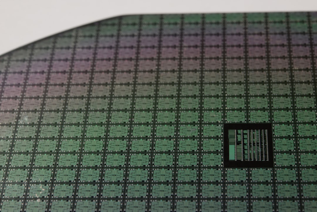
Photodetectors (PDs) and modulators (MDs) are essential components of photonic integrated circuits (PICs) and optoelectronic integrated circuits (OEICs).
The introduction of graphene and other two-dimensional materials (2DM) in the pallet of materials compatible with the PIC and OEIC industry has offered a novel paradigm in integrated PDs and MDs with a miniature footprint and ultrawide bandwidth, outperforming the standard materials and architectures. The main challenge, when graphene is deposited, is the introduction of impurities and defects that degrade device performance, especially when polymers and solvents are involved.
In particular, the wafer-scale integration of high-quality and defect free 2DM layers, without disrupting the process-line silicon foundries, has not been demonstrated. Next-2Digits aims to introduce the direct wafer-scale integration of 2DM in PICs using two additive technologies: semi dry transfer of graphene layers for full wafer scale integration and direct die processing; and Laser Digital Transfer of pristine 2DM pixels directly on the stack without the need for post-processing.
By pursuing these developments, the project seeks to enable the incorporation of 2DM in PICs and MEMS foundries, and the industrial uptake of 2DM-based devices.


