+44 (0)24 7671 8970
More publications     •     Advertise with us     •     Contact us
 
Loading...
News Article

U.S. Navy funds Mercury to develop photonic chiplet manufacturing capability

News

Mercury Systems, a technology company providing solutions for aerospace and defence, has announced an agreement with the U.S. Navy to develop manufacturing capabilities that would allow commercial photonic chiplets to accelerate edge processing in defence applications.

The Office of the Under Secretary of Defense for Research and Engineering (OUSD(R&E)) Trusted and Assured Microelectronics (T&AM) Program’s Project KANAGAWA aims to mature the domestic supply chain and manufacturing processes for multi-chip packages, where co-packaged optics are integrated with electronic integrated circuits to enable long-reach and high-bandwidth data transfer. Compared to conventional copper connections, photonics uses optical fibres to enable orders of magnitude improvement in data bandwidth at a fraction of the power needed. The promise of this technology for defence systems has been well-known for decades, but demonstrations have relied on expensive and custom approaches that are not compatible with high-volume production.

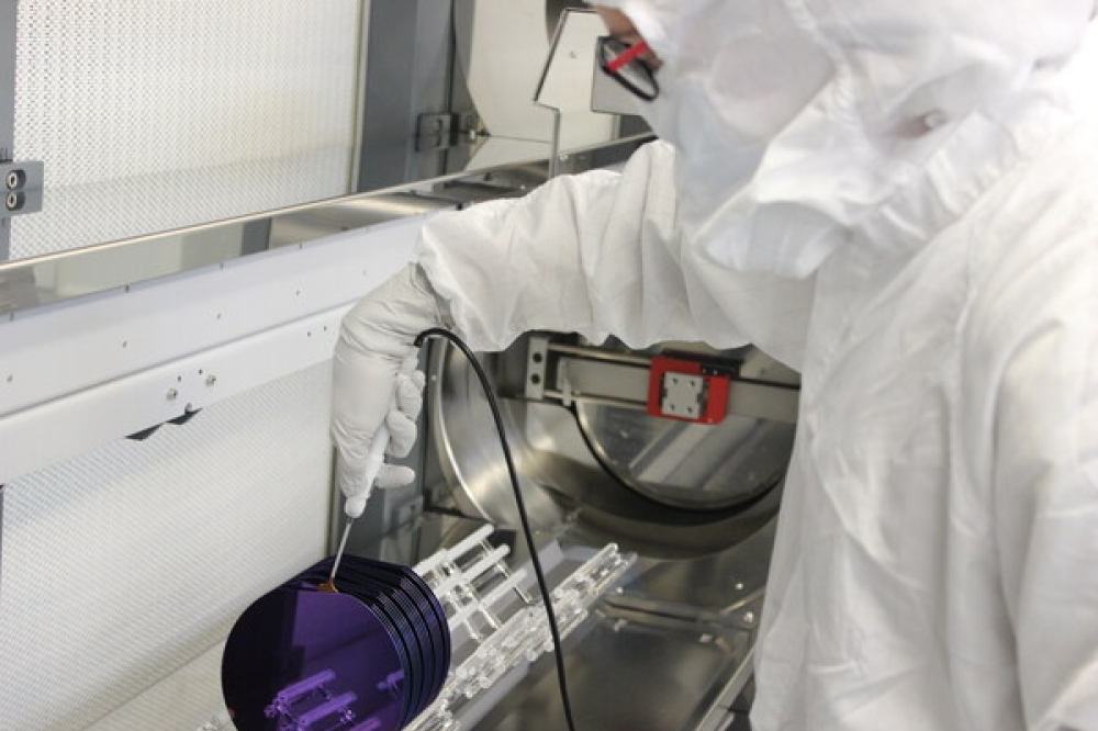
Under a $3.9 million, 17-month Other Transaction Agreement (OTA) with Naval Surface Warfare Center (NSWC) Crane Division, Mercury gains access to photonics devices developed for the commercial sector by Intel and Ayar Labs. These chiplet devices use optical technology to move data through systems such as data centres at speeds in excess of a terabyte per second. Mercury plans to develop miniaturised and ruggedised packages using photonics chiplets for defence applications to allow edge sensor data to be ingested much faster, enabling faster decision-making in next-generation radar and electronic warfare systems.

“We are excited to partner with the Navy to bring this game-changing commercial technology to the defence community,” said Tom Smelker, Mercury’s GM of Microsystems. “As we continue to drive innovation in defence microelectronics at the edge and move from board-scale to chip-scale, photonics chiplets will play a key role in advanced packaging and benefit a wide range of systems and platforms.”

Joshua Hawke, USD(R&E) RF/OE Execution Lead, added: “Breaking the data transfer bottleneck is a critical objective for the RF & Optoelectronics (RF/OE) program. This partnership with Mercury will proliferate co-packaged optics within the Defense Industrial Base and accelerate adoption of innovative technology by the warfighter.”

Samco Inc announces sale of etching systems to III-V Lab
European Innovation Council funds QuiX Quantum
Intel and Source Photonics partner on 800G transceivers
LioniX secures €1.5 million in bridge financing
A technique for 3D nanostructuring inside silicon
Senergetics wins Gerard and Anton Award
Scantinel announces new CMOS-based LiDAR chip
Project to miniaturise spectrograph wins €3.4 million
EU invests €325 million in Europe's semiconductor ecosystem
Fraunhofer IPMS developing near-infrared silicon-based photodiodes
PhotonDelta opens US office in Silicon Valley
EU funds integrated photonics for space navigation
Maryland Department of Commerce funds PIC testing and packaging facility
Lightmatter appoints Simona Jankowski as chief financial officer
scia Systems to showcase ion beam processing advances at SEMICON West
Quantifi Photonics announces Iannick Monfils as new CEO
Nokia and TTI achieve 800G on long-haul commercial network
Nokia to acquire Infinera for $2.3 billion
Advancing AI with programmable silicon photonics
Quantum PICs: Empowering designers with accurate simulations
Enabling efficient light emission and detection
Harnessing InP for applications beyond optical communications
POET wins “Best Optical AI Solution” in AI Breakthrough Awards
Intel reveals fully integrated optical I/O chiplet
People, planet, profits: a sustainable way forward for all
A bright future for the global PIC market
Atom-thin silicon-germanium sheets for integrated photonics
BAE Systems and GlobalFoundries partner on semiconductors
Wave Photonics raises £4.5 million in seed funding
Aeva to supply LiDAR for AutomatedTrain project in Germany
Black Semiconductor raises €254.4 million for graphene chips
Pooya Tadayon joins Ayar Labs

×
Search the news archive

To close this popup you can press escape or click the close icon.
Logo
×
  • 1st January 1970
  • 1st January 1970
  • 1st January 1970
  • 1st January 1970
  • 1st January 1970
  • 1st January 1970
  • 1st January 1970
  • 1st January 1970
  • View all news 22645 more articles
Logo
×
Register - Step 1

You may choose to subscribe to the PIC Magazine, the PIC Newsletter, or both. You may also request additional information if required, before submitting your application.


Please subscribe me to:


You chose the industry type of "Other"

Please enter the industry that you work in: