
Ayar Labs showcases optically-enabled Intel FPGA
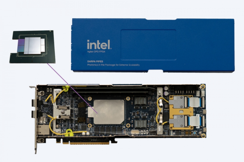
Ayar Labs, a company developing silicon photonics solutions for chip-to-chip connectivity, will showcase its in-package optical I/O solution integrated with Intel’s Agilex field-programmable gate array (FPGA) technology at the upcoming Supercomputing 2023 conference from 12-17 November in Denver. The company says that the optical FPGA, which is packaged in a common PCIe card form factor, demonstrates 5x current industry bandwidth at 5x lower power and 20x lower latency. According to Ayar Labs, it therefore has the potential to transform the high performance computing (HPC) landscape for data-intensive workloads such as generative artificial intelligence (AI) and machine learning, and support novel disaggregated compute and memory architectures.
"We’re on the cusp of a new era in high performance computing as optical I/O becomes a ‘must have’ building block for meeting the exponentially growing, data-intensive demands of emerging technologies like generative AI," said Charles Wuischpard, CEO of Ayar Labs. "Showcasing the integration of Ayar Labs’ silicon photonics and Intel’s cutting-edge FPGA technology at Supercomputing is a concrete demonstration that optical I/O has the maturity and manufacturability needed to meet these critical demands."
Ayar Labs describes the optical FPGA as consisting of two TeraPHY optical I/O chiplets that are each capable of 4 Tbps bi-directional bandwidth. These chiplets are connected to a 10 nm FPGA fabric die, the core fabric used in Intel’s Agilex FPGAs. The optical communication is powered by two SuperNova light sources, supporting 64 optical channels of communication across eight fibres on each chiplet. The company says this configuration is capable of delivering 5x the bandwidth at a fraction of the power (<5 pJ/b) and latency (5 ns per chiplet + TOF) required by current industry solutions, all critical factors for the future of high performance compute fabrics and next-generation disaggregated architectures.
"At Intel, we pursue relentless innovation with our FPGA portfolio," said Venkat Yadavalli, VP and GM of Intel’s Product Excellence Group. "With Ayar Labs’ in-package optics coupled with our FPGA fabric die, we created I/O bandwidth over 4 Tbps — far greater than what is currently possible with electrical connections. We’re looking well beyond 400G Ethernet with this capability. Optical interfaces like these have the potential to unlock huge advancements in high performance computing, AI, data centres, sensing, communications, edge, and more. Imagine what you could do with an optical interface FPGA communicating at over 4 Tbps."
This development has utilised the emerging chiplet ecosystem, combining Ayar Labs’ optical I/O chiplets developed on GlobalFoundries’ Fotonix monolithic silicon photonics platform with Intel’s FPGA and leading packaging process into a single package. Ayar Labs says that this co-packaged integration has delivered a step function in performance without changing the underlying compute silicon, illustrating the benefits of the chiplet ecosystem.


