
Scientists report integrated photodiodes on TFLN
Thin-film lithium niobate (TFLN) is often considered a promising platform for photonic integrated circuits due to its tight mode confinement, high nonlinear efficiency and wide transparency window. Chinese scientists have recently reported an ultra-wideband waveguide-coupled photodiode on the TFLN platform, achieving a 3-dB bandwidth of 110 GHz and a responsivity of 0.4 A/W at 1,550 nm wavelength.
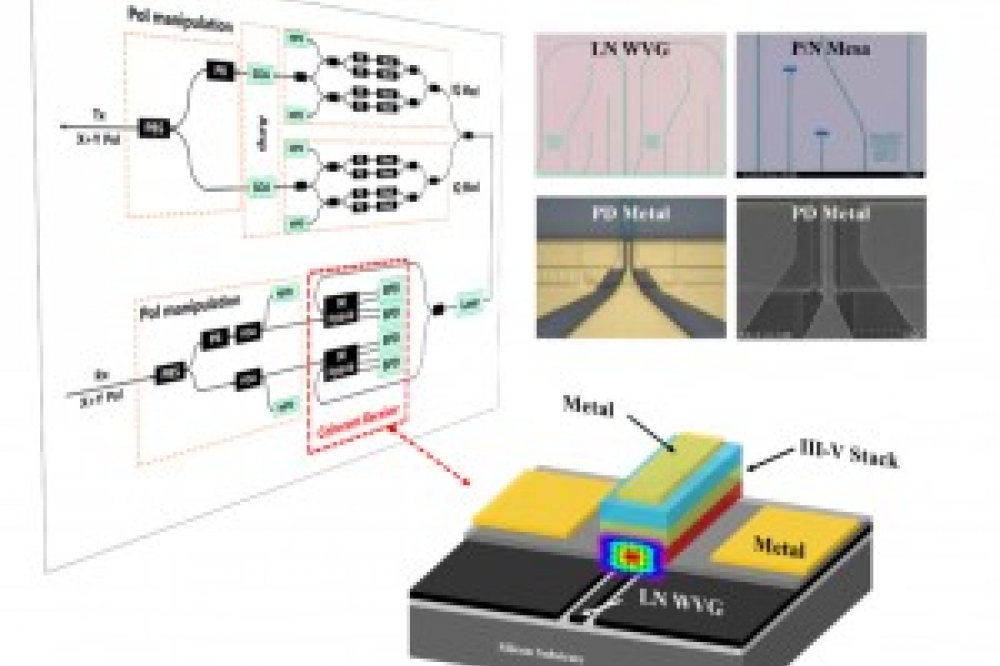
Owing to its strong electro-optic coefficient and wide transparency window, lithium niobate (LN) has become an attractive photonic material. Thin-film lithium niobate (TFLN) technology has enabled tight mode confinement and high nonlinear efficiency. Various compact integrated photonics devices have been realised on the TFLN platform, such as compact high-performance modulators, polarisation management devices, and broadband frequency comb sources. However, the inherent difficulty of creating lithium niobate light sources and photodetectors poses a challenge for the TFLN integrated photonics platform. As an essential optoelectronic component, an on-chip integrated high-performance photodetector is vital for TFLN photonic integrated chips.
In a new paper published in Light: Advanced Manufacturing, a research team, led by Professor Xiaojun Xie and Lianshan Yan from Key Laboratory of Photonic-Electric Integration and Communication-Sensing Convergence, School of Information Science and Technology, Southwest Jiaotong University, China, has reported a high-speed and high-responsivity modified uni-traveling carrier photodiode heterogeneously integrated on the TFLN platform. According to the paper, the device exhibits a 3-dB bandwidth of 110 GHz and a responsivity of 0.4 A/W at a wavelength of 1,550-nm wavelength.
The researchers described the fabrication process as being initialised by the dry etching of LN waveguides and passive devices. A hybrid etching approach was followed to form device mesa. After metal plating and lift-off, the chips were diced and polished. The epitaxial layer structure, LN waveguide geometry, and CPW pad geometry were optimised to achieve both large bandwidth and high responsivity.
To further assess the performance of the devices, the team applied them to a data transmission system, and say they successfully detected PAM4 signals at 32 Gbaud with high quality. The researchers also say they have demonstrated that the heterogeneously integrated photodiodes on the TFLN platform have the potential to be applied in the next-generation high-speed transmission systems.
According to the scientists, this work paves the way to achieving massive-scale, multi-function, and high-performance TFLN photonic integrated circuits, as well as holding promise for ultra-high-speed optical communications, high-performance integrated microwave photonics, and multi-function integrated quantum photonics


