
Photonic integration and packaging with Photonic Wire Bonding and facet-attached micro-optical elements
Fully automated solutions for seamless transitioning from prototyping to high-volume production.
By Sebastian Skacel, Laura Horan and Calin Hrelescu, Vanguard Automation
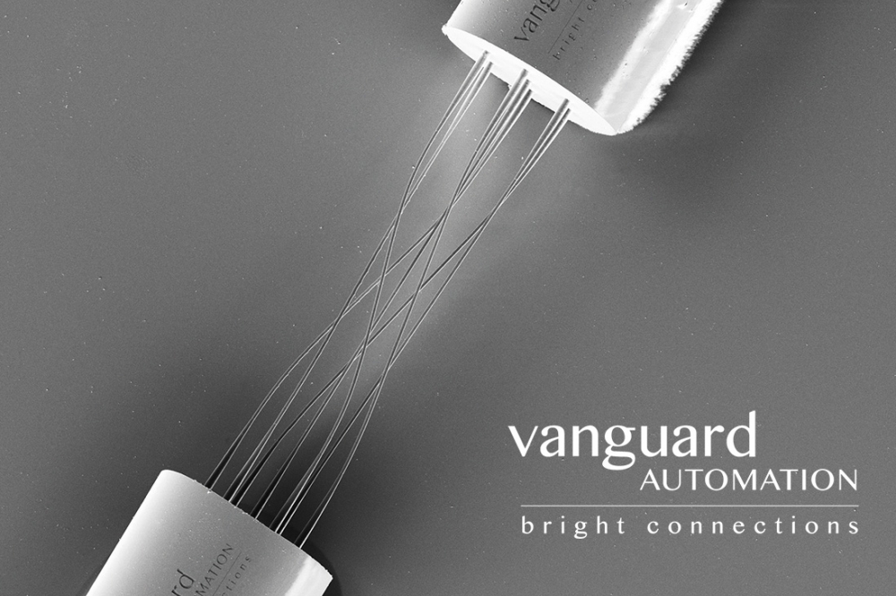
The rapid growth of photonic integrated circuits is driving the need for fast innovation, and this is made possible by the development of Photonic Wire Bonding (PWB), which creates low-loss, 3D free-form connections between optical components. Just as electrical integrated circuits have benefitted from electronic wire bonding, photonics innovations will now advance on a faster trajectory with PWB.
Built on advanced 3D nano-printing technology, PWB is inherently a fully automated process and provides a high degree of design flexibility.
Additionally, 3D nano-printing has been used for several years to fabricate facet-attached micro-optical elements on optical chips and fibres, enabling low-loss coupling with relaxed alignment tolerances and wafer-level probing of optical devices. With both PWB and facet-attached micro-optical elements in their technology portfolio, Vanguard Automation’s mission is to advance photonic packaging and assembly by providing scalable 3D nano-fabrication solutions, allowing seamless transitions from prototyping to industrial high-volume production.

Figure 1: Vanguard Symphony, Vanguard Automation’s fully automated photonic integration and packaging solution comprising the automated 3D lithography-based nano fabrication unit Sonata 1000 and the automated pre- and postprocessing unit Reprise 1000. The systems are equipped with Vanguard’s BrightWire3D software, enabling highly precise detection and on-the-fly trajectory calculations. Vanguard’s own photoresists (Vanguard VanCore series), standard process development, as well as product support and engineering services complete Vanguard’s solution from prototyping to high-volume production.
Today’s packaging and assembly challenges arise from the need to integrate various optical components from different material platforms. Take, for example, a hybrid module, comprising indium phosphite-based active devices such as lasers or semiconductor optical amplifiers, passive devices made from silicon, silicon nitride or lithium niobate, as well as photodiodes and single-mode or polarization-maintaining fibres. Packaging such a module entails an integration challenge due to the very specific optical properties of each component. To be viable for industrial mass production, packaging and integration solutions must address and solve the challenges that these specific optical properties present.
To reduce coupling loss when combining different photonic devices, the specific mode field profiles have to be matched and the devices have to be aligned very precisely. In industrial mass production, processes such as mode matching and alignment must be fast and reproducible since speed and yield determine the cost of the product. Additionally, the packaged assemblies need to be reliable under various environmental conditions which are specific to their applications.
Although the application-specific conditions, such as the environmental conditions that the packaged assemblies must withstand, may vary considerably, the fundamental requirements of efficient and reliable packaging hold true for a large range of application areas such as telecommunications and datacom, 3D sensing, LiDAR and quantum applications. Hence, even though photonic devices used for such specific applications are made with sophisticated processes from sometimes exotic material platforms, the optical packaging or integration process remains in most cases the biggest cost driver.
Vanguard Automation solves these challenges with its fully automated solution portfolio: the Vanguard Symphony comprising two systems, one for the fabrication of PWB as well as facet-attached micro-optical elements (Vanguard Sonata 1000), and one for postprocessing of connected optical assemblies completing the fully automated packaging process (Vanguard Reprise 1000). This solution includes Vanguard’s Brightwire3D software for automated, highly precise (accuracy < 100 nm) interface detection as well as on-the-fly calculation of optimal PWB trajectories, and dedicated photoresists tailored to meet strict industrial reliability requirements (Vanguard VanCore series). Vanguard Automation also provides standard processes as well as engineering service and support to enable customers to advance quickly from prototyping phases to high-volume production (see Fig. 1).
Over the past years, the number of Vanguard technology adopters and ecosystem partners has rapidly increased (see Fig. 2). Our customers and partners have used Vanguard’s PWB and facet-attached micro-optical elements technology in many applications solving the various challenges of hybrid module packaging and integration.

Figure 2: List of Vanguard Automation’s technology users and ecosystem partners which can be disclosed at the time of publication.
In the data centre, telecommunication, and artificial intelligence markets Vanguard’s customers[1] have utilized innovative PWB processes working on various material platforms, such as silicon, silicon nitride, indium phosphite, and lithium niobate to advance the concept of hybrid integration[1] (see Fig. 3). Offering the unique advantage of using only one coupling Process Design Kit (PDK) to couple to other types of optical components, Vanguard’s technology portfolio is compatible with all academic and commercial foundries. Consequently, foundries can avoid having to create complex spot size converters.[2]
Since the Vanguard technology can work with simple inverse tapered edge couplers realised by stepper lithography, the chip real estate used for sophisticated couplers can be reduced substantially, paving the way towards a novel and more universal standard for optical coupling. PWB has been utilized for self-injection-locked Kerr soliton microcombs and lasers with sub-100Hz linewidth. [3, 4] In the field of quantum applications, PWB has been successfully tested in ultra-low-temperature experiments.[5]

Figure 3: Examples of photonic wire bonds (PWBs) demonstrating low loss connectivity solutions for active and passive devices from various foundries. (left) AMF (Si) chip with 1.5dB loss and (centre) AIM (SiN) chip with 1.7dB loss per PWB. (right) Mentech (InP) laser diode array with 1.5dB loss per PWB.

Figure 4: Vanguard Automation’s industrial grade facet-attached micro-optical elements technology compatible with a large variety of applications and widely tested under industry standards.
Furthermore, Vanguard Automation’s facet-attached micro-optical elements have demonstrated improved efficiencies for High-Bandwidth Coherent Driver Modulators (HB-CDM) [2]. Vanguard’s dedicated photoresists series VanCore, tailored to meet strict industrial reliability requirements, is proven to be reliable under the harshest environmental conditions [2]. (see Fig. 4). The facet-attached micro-optical elements have created a powerful platform for electro-optical engines for transceivers, co-packaged optics, light engines, and sensing devices [6].
Incorporating Vanguard’s technology improves the coupling efficiency of light as it passes from one photonic device to another, which in turn reduces the power consumption of the combined solution (see Fig. 3 & 4). The precise alignment and printing of the facet-attached micro-optical elements at the wafer level enables significant scalability and enhances the ability to address new applications[6, 7, 8, 9]. Vanguard’s facet-attached micro-optical elements technology has already been successfully used in LiDAR applications for beam shaping elements [10] and in quantum applications to increase the effective collection area of superconducting nanowire single-photon detectors (SNSPD), thereby overcoming a fundamental design conflict of such devices [11].
Due to its complementary technology portfolio combining PWB and facet-attached micro-optical elements, Vanguard Automation offers volume production customers a simplified path for incorporating the Vanguard technology into their production chain. In the first instance, Vanguard technology can be included in hybrid approaches together with conventional technologies such as active alignment [2] to improve coupling efficiencies and yield. This approach does not imply any major changes to the chain of process steps in production.
Secondly, beam-expanding micro-lenses can be implemented in products to ease the positioning tolerance of PICs and other optical components such as InP-lasers and fibres, thus relaxing alignment tolerances to such a degree that passive assembly becomes a viable process[9]. Finally, the full disruptive potential for photonic integration and packaging can be introduced by incorporating PWB into the product design. This supports a shift towards standard pick and placing of all components of a hybrid multi-chip assembly with very relaxed placement tolerances, while simultaneously ensuring high coupling efficiency and high yields, as well as fast manufacturing and high package density.
In summary, Vanguard’s PWB technology enables the combination of the complementary strengths of different optical integration platforms in advanced photonic multi-chip modules leading to compactness with high performance and design flexibility. Vanguard’s photonic integration solution portfolio is completed with facet-attached micro-optical elements on optical chips and fibres, allowing for low-loss coupling with high alignment tolerances and for wafer-level probing of optical devices. The fully automated, highly reproducible, and reliable Vanguard Symphony solution is already being used by research and industry customers targeting next-generation photonic integration and packaging.
[1] ‘Optical Product Innovations with Photonic Wire Bonding - Lightwave webinar’. https://www.aeponyx.com/lightwave-webinar
[2] Y. Mizuno et al., ‘Low Insertion Loss 128-Gbaud HB-CDM with 3D-Printed Spot Size Converter Integrated InP-based Modulator’, in 2023 OFC (2023), paper Th2A.8, doi: 10.1364/OFC.2023.Th2A.8.
[3] Y. Chen et al., ‘Self-Injection-Locked Kerr Soliton Microcombs With Photonic Wire Bonds For Use in Terahertz Communications’, in CLEO 2023 (2023), paper STh3J.1, doi: 10.1364/CLEO_SI.2023.STh3J.1.
[4] Y. Chen et al., ‘Frequency-Agile Self-Injection-Locked Lasers With sub-100 Hz Linewidth based on In-Package Photonic Wire Bonds’, in CLEO 2023 (2023), paper STu4P.4, doi: 10.1364/CLEO_SI.2023.STu4P.4.
[5] B. Lin, D. Witt, J. F. Young, and L. Chrostowski, ‘Cryogenic Optical Packaging Using Photonic Wire Bonds’. arXiv, 2023, doi: 10.48550/arXiv.2307.07496.
[6] ‘POET Technologies and Vanguard Automation Collaborate on Solutions for Co-packaged Optics’. https://poet-technologies.com/news/2023-mar-6.html
[7] Y. Xu et al., ‘3D-printed facet-attached microlenses for advanced photonic system assembly’, Light Adv. Manuf., 4 (1), 1–17, 2023, doi: 10.37188/lam.2023.003.
[8] P. Maier et al., ‘3D-printed facet-attached optical elements for connecting VCSEL and photodiodes to fiber arrays and multi-core fibers’, Opt. Express, 30 (26), 46602–46625, 2022, doi: 10.1364/OE.470676.
[9] ‘H2020 Ophellia: On-chip PHotonics Erbium-doped Laser for LIdar Applications’. https://lidar-ophellia.eu
[10] S. Singer et al., ‘3D-printed facet-attached optical elements for beam shaping in optical phased arrays’, Opt. Express, 30 (26), 46564–46574, 2022, doi: 10.1364/OE.456952.
[11] Y. Xu et al., ‘Superconducting nanowire single-photon detector with 3D-printed free-form microlenses’, Opt. Express, 29 (17), 27708–27731, 2021, doi: 10.1364/OE.427639.


