
From processing and computing to sensing
The recent CEA-Leti Innovation Days provided a great opportunity to
learn about some of the very latest developments and research being
undertaken in the semiconductor industry, covering such topics as
quantum computing, sustainable electronics, cybersecurity and memory for
edge computing. There was a dedicated session on Photonics: Data and
Sensing, which looked at photonics for computing and communications as
well as integrated photonics for biomedical and chemical sensing
applications.
Eléonore Hardy, business developer at CEA-Leti,
co-chaired the workshop and here she provides an overview of the topics
and technologies discussed, in conversation with Philip Alsop,
contributing editor to PIC Magazine.
From 27-29 June, the French technology research institute CEA-Leti held its Innovation Days – an annual three-day conference that brings together technology leaders from around the world to share their latest and most exciting developments. This year’s event hosted a dedicated photonics workshop called “From Processing and Computing to Sensing".
PA : At the recent CEA-Leti Innovation Days, there was a workshop on photonics, which you co-chaired. Could you tell me a bit about how the day went?
EH: This workshop went really smoothly. I was particularly happy with the attendance. In the morning, we had a session dedicated to communications and computing applications for photonics, and in the afternoon, we were really focusing on sensing applications. We could not cover everything in one day, but we had very interesting talks with people from both industry and research. What I found really nice about this session was seeing the different points of view of our different speakers. Some speakers, like STMicroelectronics (ST), were giving foundry perspectives, and Hewlett Packard Enterprise (HPE), for example, was giving a system perspective on photonics, so it was a very rich discussion. We also had panel discussions at the end of each session to have questions from the audience to our speakers.
PA: The headline talk was “Photonics 2.0 and Applications.” I'm sure that is quite a big topic, but can you give us some flavour of that high level overview of photonics? What did you cover?
EH: The aim was to start the session with a really broad overview of photonics and its applications. We gave the mic to Frederic Boeuf, who is the technical director of technology R&D for photonics at ST. He gave a vision of the possibilities given by silicon photonics platforms for different applications. He covered, of course, datacom applications, because this is really what we are facing today: a big amount of silicon photonics really going into all parts of the data centres, not only for interconnects between servers, but also between data centres, and now coming closer and closer to the chip. He talked about the applications for quantum communications and quantum computing, biosensing, LiDAR chips for the automotive industry, high performance computing (HPC) and also depth sensing. These can all really be pushed forward thanks to silicon photonics. Then he also gave an overview of what ST’s photonics platform can do for those applications, in particular for communications, the advantages of this platform and also what would be the next step for it.
At the end, he reviewed one very interesting point, which is the need for more advanced modulators for HPC, for communication, and for many applications. He compared different versions of modulators we can see today in papers, from very classical ones to more advanced ones. He also discussed at the very end how to integrate new materials in this platform, because we know silicon is not enough. We also need to have other materials brought into the platform, like III-V materials, of course, for lasers. But there are other integrations that are really interesting, like InGaAsP materials, and also BTO and lithium niobate. So it was a very good start for the morning.
PA: Just to pick up on something, it’s been suggested that photonics has quite an exciting future, particularly when it comes to energy efficiency. Was there any discussion during the day of how much of an impact photonics can make when it comes to energy efficiency?
During the Innovation Days, we had a very specific session on sustainability. Energy consumption is in everyone’s mind, and in photonics, as well, we have this in mind. It's important to find a way to decrease the consumption of data centres, and yes, photonics can help greatly in this change. But also looking at computing, when you talk about AI and all the needs for these new AI systems, you see that the energy consumption is incredibly high. We had a talk from Thomas Van Vaerenbergh from HPE about how photonics can help, from the interconnects to the core of the computing processors. He gave a view of the energy consumption of those processors and how photonics could really help decrease the consumption of those new computing architectures.
PA: The next presentation was to do with interposer optical communications. Could you give us a flavour of what was covered?
EH: This talk was given by Yvain Thonnart from CEA-List, who has been working on computing architectures for years. He's one of our best experts in the field, and so he really showed us how there is a big need for interposers, for HPC in particular, and why basic silicon interposers will not be enough for many reasons, like latency and energy consumption. He showed us how we could move from silicon interposers to active silicon photonics interposers that could really help in reducing the latency and the energy consumption of those architectures, by having denser on-chip interconnects with lower latency routing.
What he wanted to show is that photonics really can help scale out the interposers, allowing a routing with very low latency and low power. We have made a proof of concept of this at CEA-Leti. We are doing the tests currently, which shows this is something we can do for real and we can scale into production in the coming years.
PA: The next topic for discussion was photonic neuromorphic accelerators. Could you tell us a bit about that presentation?
EH: This presentation was made by Thomas van Vaerenbergh from HPE, who has been working on photonics for years, but also electronics. He worked on a road for optical HPC interconnects, but also on new architectures based on neuromorphic accelerators. This is a very different way to think about the next generation of accelerators. Nowadays we are focusing more on digital computing, but analogue computing is also a very interesting possibility for the future, to reduce once again the energy consumption. Thomas gave us a flavour of what photonics can do for digital computing, and also for analogue computing. He showed us the great performances that can allow photonics for machine learning accelerators.
The maturity level is still very low today for that, but we are talking about what could be next in ten years from now. And we need to prepare it today, so it was very exciting from this point of view. Thomas also tried to highlight the need for a better structure for the photonics community, to have people really able to understand each other and to have a full supply chain ready to scale up this technology.
PA: Next there was a talk about CEA-Leti’s own silicon photonics platform, so it would be good to understand what that is and where that fits within the photonics landscape.
EH: We have had a silicon photonics platform at CEA-Leti for nearly 20 years now, so we started very early in those developments. For years we worked on an 8” silicon photonics platform, which was standard. But a few years ago we moved to a 12” silicon photonics platform for many reasons, because we saw that big foundries like ST, for example, are in 12”. We need to be compatible with those very performant platforms to bring the technology for those 12” volume foundries. Also, in 12” usually you have better silicon-on-insulator (SOI) uniformity, so a better yield at the end. And you can also take advantage of immersion lithography in 12”, meaning that you can go to smaller feature sizes. The smallest feature size we usually do in 12” is around 40-60 nm for our projects. That is much better than what you can get with an 8” platform. So we developed a standard silicon photonics platform that is aimed at developing new technologies for photonics, bringing in new materials, like III-V, of course. We have worked on collective die-to-wafer bonding of III-V materials for lasers and semiconductor optical amplifiers (SOAs) for years.
We launched a startup company a few years ago, Scintil Photonics. And we also work on new materials like NbN, which is a superconductive material, which is very useful when you look at SNSPDs, or single-photon detectors needed for quantum applications. We also integrate lithium niobates nowadays by bonding, and we also work on BTO integration with Lumiphase in Switzerland. So we have a very versatile platform. This is a good field for us to work on new materials and new integrations, to find the perfect new components for the future, to then transfer them to volume foundries.
PA: Picking up on that point, the morning ended with a panel discussion about the likely or the predicted impact of photonics. Everyone will have their own view as to where and how and when, but can you give us a flavour of that discussion and maybe even your own thoughts as to where it's going to show the most or the quickest return, or just how the landscape might be developing.
EH: We had a very fruitful panel discussion. I would say what remains very important is datacom is still mainstream today for photonics, no question about it. But we have been seeing, of course, for years, a big trend to explore new applications. When you work on a photonics platform, usually you can cover more than one application with the same platform, so the versatility of silicon photonics is interesting for exploring new applications.
The morning was really focused on the advantages for computing. A highlight in the panel session was that photonics is getting closer to the cores. That’s a reality because of low latency and low power consumption again. But there is also a need to really look at photonics for a new style, a new way of computing, which Thomas from HPE spoke about in his talk on analogue computing and Benoît Charbonnier, researcher at CEA-Leti, in his talk on Neuromorphic photonics for tomorrow’s AI. For sure,photonics is also a big enabler for AI for the future, so that was a perspective we had during this panel session.
Also, when looking at material integration and foundry perspectives, working only with silicon or silicon nitride is not enough. All foundries need to look at the best integrations of materials like lithium niobate, BTO, III-V materials. This is a big challenge for future developments.
PA:The afternoon moved more to the sensors side of things. One of the first talks was about miniaturisation of mid-IR sensors. Could you talk through what happened there?
EH: This talk was given by Badhise Ben Bakir, a research engineer at CEA-Leti and he focused on quantum cascade lasers and the miniaturisation of mid-IR sensors. We have demonstrated very nice sensors in the past, and we are working on the next generations, integrating even further those sensors. The talk gave a flavour of how we work on the integration of III-V on silicon for quantum cascade lasers, especially for multigas sensors based on different technologies, such as photoacoustic detections, but also photonic integrated circuits and the QCL quantum cascade lasers integration, so Badhise talked about chemical sensing. What is really nice with photonics is that you can miniaturise the devices, but you can also target very performant devices, so this is perfect for the next generation of gas sensors. At the end he gave a view of the possibilities in mid-IR for other applications as well. He showed how we can handle the integration of III-V on silicon and the results of our quantum cascade lasers.
He also talked about the work we do in the IRT Nanoelec Consortium, which is a French consortium. We have a photonics programme with Siemens, STMicroelectronics, Almae and CNRS, so he talked about this consortium and how we developed the hybridization of III-V and silicon for new functionalities.
PA:The next talk was to do with wearables, like non-invasive biomolecule sensors. I'm intrigued about what's going on with that these days.
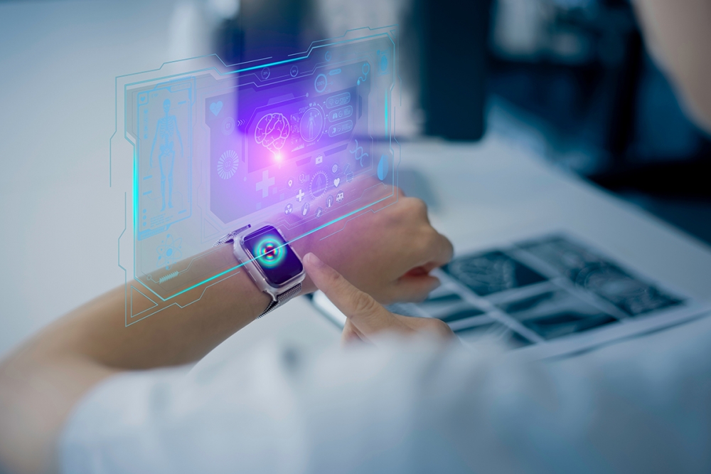
EH: We were very lucky to have Hélène Lefebvre, CEO of the startup ECLYPIA. ECLYPIA was in stealth mode for two years, and last May they decided to share their developments during Medi’nov, a conference and show in Lyon about medical developments. ECLYPIA is a startup company bringing a new generation of non-invasive continuous glucose monitoring. The developments they are making are really going to change the lives of people with diabetes. Hélène presented their latest developments and we were very lucky to have them for this session.
PA: Am I right in thinking Admir is another startup company that shared what they're doing technology-wise?
EH: Admir is a young startup spinoff of CEA-Leti and Laurent Duraffourg, the CEO, came to present their multispectral spectroscopic lensless imaging system. This is a brillant system they are developing and once again it is very useful for people’s health because it's a system that you can use for ultrafast cancer diagnostics. Laurent introduced the concept of how the technology works, not only for the detection of cancer, but also for microbiology applications like the analysis of water or food to detect bacteria, and also the detection of microplastics in water. So these are very important topics as well for our future. The talk introduced the technology, the possibilities for those different applications and how they are developing this, thanks to the collaboration of doctors they are working with. Once again, it was a mid-IR photonic platform that is used for those developments. This is really the link between all the talks we had in the afternoon: how those mid-IR photonic platforms can help for medical applications.
PA:The final technical presentation before the panel discussion was to do with Mach-Zehnder interferometers. Please tell us what that was all about.
EH: This presentation was by Loïc Laplatine, who is a researcher at CEA-Leti. We have this very nice silicon nitride photonics platform we have been developing for years, and based on that there were developments based on Mach-Zehnder interferometers for biosensing and olfactometry. In fact, we have a startup company called Aryballe that was mentioned during this talk. Loïc showed the results of Aryballe’s NeOse products for odour analysis. This is quite incredible, but thanks to a photonic chip, you can have analysis of the odours around you and you can find applications for this in many different areas. It can be, of course, for the perfume industry, but also for the food industry and even the automotive industry. When you rent cars, you need to make sure that the car you are renting will have a nice odour in it. So we had this presentation from Loïc to show how it works, how we make those chips and the functionalisation of those chips. He showed how we work with the microfluidic integration as well, because the chip itself is not enough; once you have your photonic chip, you also need to have the electronics and the microfluidic system to have the flow of gas going around. At the end, Loïc showed the applications for biosensing based on photonic integrated circuits with VCSELs as the light source. It could also be used in environmental sensing and monitoring, to detect bacteria in rivers, for example.
PA: From what you've said, it sounds as if there's plenty of work already going on in sensing applications, but it can be a time consuming process meeting regulatory requirements and/or to gain the trust of the users?
This is a big challenge for biomedical applications, because you need to take the time to go through all the regulations and this is a long process. Those startup companies are really doing a great job in this industry, but you need to also be patient to go through all the steps to qualify. You also need to go through some steps to convince end users that the new devices are reliable, and to show patients and doctors that the equipment is bringing a plus to their life. So, yes, they discussed the challenges faced by startups for biomedical applications.
If you had to choose one or two things to take away from the day, anything that brought you up short and made you feel “wow, that's amazing,” or “I didn't know that,” what would they be?
That's a very tough question. I would say from the morning session, my takeaway is that we are getting more and more mature silicon photonics platforms, which is very good news, because now more and more companies can start really to put their hands on those platforms, to develop new circuits and new solutions. But there are still lots of challenges for new material integration, which is good news. We still have work to do.
My takeaway from the afternoon would be: “wow, how fantastic our world can be thanks to photonics for medical applications.” I saw in the presentation from Admir how much time you can save for cancer diagnostics, and in the presentation from Hélène from ECLYPIA how you can really change the life of millions, billions of people on Earth, thanks to nice, accurate sensors that you can handle discreetly in your watch, for example. We are bringing huge contributions to our future, so this is very exciting for people working in photonics to see we are doing something very useful.
PA: It's been pleasure to chat to you and thank you so much for bringing alive the workshop in the way you have.
EH: My pleasure. Thank you and see you next year at the next Innovation days.


