
Photonic integrated circuit packaging, from prototype to production scale-up
Packaging photonic integrated circuits (PICs) can be complicated and
expensive, but using standardized components and automated assembly
processes in the testing and development stages can significantly reduce
costs and improve the final product.
By Gijs van Ouwerkerk, Marketing and Communication Specialist, PHIX Photonics Assembly
Packaging photonic integrated circuits (PICs) into functional optoelectronic devices is often complex and costly. Bringing together optical and electrical interfacing, thermal management, mechanical support and sometimes even chemical sealing, PIC packaging requires a multi-disciplinary team of experts. On top of that, standardization within the industry is lacking at the front-end, where many different PIC material platforms exist that often need to be co-packaged to combine their strengths.
These factors mean that packaging can swallow a large share of the total costs of PIC-based optoelectronic module development. But there is also an opportunity here: cost savings in this area will have a large positive effect on total expenses. This article will discuss an approach to PIC packaging that minimizes costs and maximizes performance of the end product by considering product design, manufacturing equipment sourcing and process development in parallel and at a system design level.
As the PIC-based optoelectronic device matures from its prototyping phase towards a product manufactured in volume, it is inevitable that the design of the PIC and its surrounding module will go through a series of transformations. Paradoxically, the article will show that designing effectively for volume production actually means starting with a prototype package. Even when manufacturing volumes are low at first, automated assembly can play a key role in keeping the cost down.
The need for prototype packaging
The first step in the development of a PIC-based device is to perform characterization of the first manufactured chips, often produced on multi-project wafers (MPWs). The designer could be interested in measuring variations between dies, fine-tuning waveguide tapers, or comparing different chip designs with each other. Although this can be done by connecting electrical and optical probes to the bare die, there are severe downsides to this. First, the temporary optical interfaces obtained in this way are not stable, so the data about the performance of the chip is polluted by the fluctuating performance of the interface. Secondly, environmental temperature changes also affect the chip’s properties and introduce additional performance fluctuations.
To drastically reduce these variations, using a simple open architecture prototype package makes a lot of sense. Here, the electrical connections are wire bonded out to simple printed circuit boards (PCBs), the optical signals are coupled to fibre arrays secured with index matching epoxy and stress reliefs, and a thermal management system is installed.
Temperature management can be passive, with a large copper mount acting as a heatsink, or active, by using a thermoelectric cooler (TEC) in combination with a TEC controller and thermistor fitted inside the copper mount.
PIC characterization package with fibre arrays, electrical fan-outs and a thermoelectric cooling solution.
This module is suitable not only for PIC characterization, but also for device characterization and system integration, enabling demonstrations outside of a laboratory environment. Since the device prototyping phase usually involves multiple design iterations of the chip and/or module, each requiring new packaging, it’s important to keep packaging costs and turnaround times as low as possible. The way to do this is to work with standardized off-the-shelf packaging building blocks and standardized automated assembly processes as much as possible. This avoids custom package design, parts, equipment, tooling and (manual) processes. Custom packaging of small series is difficult to automate, expensive, time-consuming, carries more risk, and may involve parts for which there is a minimum order quantity (MOQ). It should be put off for as long as possible, until the PIC design is ready for assembly into qualification modules in higher volumes.
How to minimize prototyping time and costs
There are several ways to design the PIC to work with standardized building blocks and production processes for easy prototyping. For example, PHIX has developed prototype packaging solutions that use waveguide alignment loops, electrical bond pad pitches compatible with standard PCBs, and the packaging foundry’s standard housings and accessories.
Waveguide alignment loops
Waveguide alignment loops are extra waveguides, not used as part of the functional structures on the PIC, that enable active alignment during the assembly of the optical interface, particularly the attachment of fibre arrays. Active alignment achieves the best possible coupling efficiency for optical assembly processes in prototype PIC packaging. Crucially, the presence of waveguide alignment loops allows the packaging foundry to use standardized and automated alignment routines involving calibrated light sources and detectors.

Waveguide alignment loops in a PIC to aid edge coupling of a fibre array.
Performing active alignment without these loops would mean using probes to activate the functionality of the PIC, for example, by driving gain elements and measuring photodiode currents. These probes are chip-specific and therefore would need to be custom-designed and manufactured for each project, requiring non-recurring engineering (NRE) with added development time and cost. Furthermore, using the functional structures on the PIC as part of alignment routines pollutes the assembly performance data with the product performance data, making this method of process control monitoring less reliable.
Although waveguide alignment loops occupy some space on the PIC and require additional fibres, they compensate for this added cost by making the manufacturing process during the prototyping packaging phase much more affordable and reliable.
Bond pad pitches compatible with standard PCBs
In PIC prototype packaging, where making flip chip electrical connections using redistribution layers and land or ball grid arrays (LGAs or BGAs) is not yet feasible, it’s common to place direct current (DC) bond pads near the edges of the PIC and wire bond out to the neighbouring PCB or housing. Due to the high accuracy of the lithographic etching processes of PIC foundries and the desire to make PICs as small as possible, there is a tendency to place these bond pads very close to each other on the PIC surface. Such small bond pad pitches, however, can be detrimental to achieving low costs and short lead times in prototype packaging.
The reason for this is incompatibility between the PICs and standard PCBs. To prevent wire bonds from shorting or sagging, they need to be as short and as parallel as possible. Ideally, they should cross straight over from the PIC to the PCB, so the bond pad pitch on the PIC needs to match that on the PCB. But, since most standard PCB suppliers only support pitches down to 200 µm, while pitches on PICs are sometimes chosen to be as small as 70 µm, there can be problematic mismatches.

Wire bonds crossing over straight and parallel from a PIC to a PCB.
A packaging foundry can deal with small bond pad pitches on the PIC by choosing thin film ceramic or organic interposers from specialized suppliers, or by using staggered vias for distributing the signals to different layers of the PCB. However, these solutions are very costly due to the NRE and expensive components they require. Furthermore, they make process automation much more difficult. Instead, choosing a sufficiently large bond pad pitch on the PIC during the packaging prototyping phase can ensure compatibility with standard low-cost PCBs, significantly reducing the cost and lead time of the prototype packages.
Using standard packaging solutions
Another way to reduce the level of customization involved in creating a PIC package is to make use of standardized packaging solutions. PHIX offers solutions that consist of standard off-the-shelf building blocks, but still provide flexibility and design freedom. This approach allows the packaging foundry to leverage previous engineering efforts and keep standard parts in stock, thus eliminating the problem of minimum order quantities. This method also allows for the use of standardized (semi-)automated assembly processes, ensuring a cost-effective prototyping phase with short lead times. 
A standard fan-out solution for a large area goldbox module, providing DC and RF connections.
Butterfly and goldbox housings have many of the same advantages, but they require custom interiors. They are worth considering if radio frequency (RF) electrical signals are used. Besides prototyping they are also suitable for qualification packages in higher production volumes. Standard electrical fan-out solutions offered by packaging foundries allow convenient connectivity for device characterization and system integration tests.

Building blocks of a standard PIC packaging housing, with copper mount, fibre array strain reliefs, and standard PCBs.
Design at system level
Designing a PIC based optoelectronic module is a multidisciplinary activity where PIC and module design must be in harmony with process development and manufacturing equipment. PIC packaging therefore needs to be approached with an eagle eye view of the system, where product performance is weighed with cost and ease of scale-up.
The use of waveguide alignment loops and the choice of a DC bond pad pitch compatible with wire bonding to standard PCBs are good examples of this system-level approach. Some other areas of PIC design that require attention in this regard include mode field matching and power budget.
Mode field matching
Significant optical losses can be caused by mode field mismatches between optical components being assembled. This is of particular concern when edge coupling fibre arrays (with typical mode fields of 10 µm) to PIC waveguides (with mode fields that can be as low as 1 µm). The best coupling performance is obtained if the mode fields of the two components match as closely as possible at the interface. In addition, the mode fields at the interface should be as large as possible, to reduce the influence of manufacturing tolerances on the coupling losses.
Traditional solutions for mode field matching between optical fibres and PICs involve lensed or tapered fibres with high numerical apertures. This approach works well for single fibre attachments but, when applied to multichannel fibre arrays, it poses significant alignment challenges and makes the assembly process difficult to automate. As dense PICs with high channel counts become the norm, these individual fibre treatments are quickly becoming obsolete for mode field matching.
Spot size converters (SSCs), on the other hand, are mode field matching solutions that scale well with channel count. They are waveguide tapers that resize and/or reshape the mode field near the optical coupling interface. SSCs perform best and are most cost-effective when they are a functional building block on the PIC itself. The availability of on-chip SSCs depends on the PIC platform and whether or not the PIC foundry supports it. If an on-chip SSC is not available or if it does not eliminate the entire mode field mismatch, then the packaging foundry may offer other solutions, such as off-chip SSCs pre-attached to a fibre array. These are typically made from ion-exchanged glass or silicon nitride and have lithographically defined tapered waveguides. They can be attached to fibre arrays using automated active alignment processes, even in small volumes.
Multi-channel spot size converter attached to a fibre array.
Power budgeting
Another example of good system-level design is to consider the power budget for each component or interface in the package. It’s very difficult to avoid introducing small losses in many places in the design, starting at the optical structures on the chip and moving through all the components and interfaces. These losses should be considered in the context of the whole system, in order to choose the right components and assembly processes needed for the desired functionality and performance.
Packaging foundries are capable of assembling components at high accuracies and with minimal losses, but the engineering, processes and equipment this requires come at a cost and may be difficult to scale to volume production. For certain PIC applications, such as in quantum or astrophotonics markets, where every decibel of loss matters and manufacturing volumes are relatively low, the higher costs of top-quality interfaces may be acceptable. However, if the device is intended to scale to high volumes, it is important to add some margin to the power budget in order to relax assembly constraints and allow a more affordable and scalable automated manufacturing process. A sufficient power margin gives the packaging foundry some freedom to design for manufacturability and cost-effectiveness, rather than having to focus purely on achieving maximum performance.
The PIC designer should be aware that, besides mode field matching and power budgeting, there are many other recommended design practices that favour manufacturability and cost-effective scaling. It is recommended that designers get in touch with a packaging foundry early and benefit from their experience.
The road to volume production
The previous sections described a cost-effective iterative prototyping phase for the PIC and the device, with fast turnaround times. Having approached the design of the PIC-based module at system level, the full playing field of design parameters has come into view.
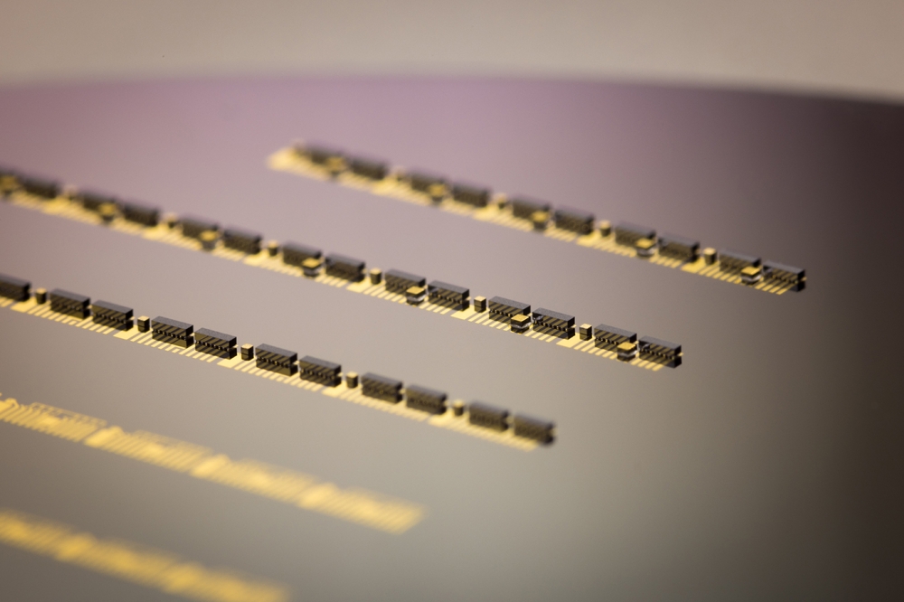
The next phase in the volume scale-up is to develop a qualification package that is optimized for consistent performance and low cost per unit. At this stage it starts to make sense for the packaging foundry to make investments in custom parts, tooling, processes, and perhaps even equipment. Since the structures on the PIC now have a stable and well-known performance, they can be used for active alignment routines that no longer require waveguide alignment loops and extra fibres. Flip chip assembly of electrical components may become a feasible alternative to wire bonding, because it will become possible at wafer level instead of at chip level. These considerations can now lead to a minimization of chip area without compromising the assembly processes or performance.
Flip chip assembly of electronic components onto silicon nitride at wafer level.
The qualification package and its contents may require sealing and be subject to reliability testing and yield optimization. Once the PIC design is frozen, the final volume package can be defined. Then, if the manufacturing volumes are sufficiently high, the packaging foundry can transition from batch level automation to the deployment of a dedicated, fully automated production line for the product.
Conclusion
Navigating towards volume packaging of an optoelectronic device in the quickest and most cost-effective way revolves around two main principles. Firstly, the PIC design should be approached at a system level, considering all aspects of the optoelectronic module and its manufacturing. Secondly, the PIC design and its packaging should be adapted to the state of maturity of the product, putting off the use of customized design, components, and processes for as long as possible.
This approach requires the PIC designer and the packaging foundry to work closely together. The PIC designer should seek out this collaboration as early as possible in the design process. It’s the responsibility of the foundry, on the other hand, to offer multidisciplinary engineering support to promote PIC designs that are optimized for cost-effective packaging, and to assist in a smooth scale-up from prototype to automated volume manufacturing.


