Component viability risks bursting the quantum bubble

To speed the arrival of quantum technologies, the incredibly
demanding compound semiconductor devices that lie at the heart of them
need to be produced on high-volume platforms.
BY DENISE POWELL AND
WYN MEREDITH FROM THE COMPOUND SEMICONDUCTOR CENTRE, SAMUEL SHUTTS FROM
CARDIFF UNIVERSITY, MOHAMED MISSOUS FROM THE INTEGRATED COMPOUND
SEMICONDUCTORS, MOHSIN HAJI FROM THE NATIONAL PHYSICAL LABORATORY AND
CHRIS MEADOWS FROM CSCONNECTED
There is no doubt that quantum technologies have the potential to revolutionise every sector we can think of. Their impact will include: highly accurate navigation, enabled by quantum gyroscopes; GNSS-free communications, underpinned by atomic clocks; ultra-secure communications, via quantum key distribution; improved manufacturing control and timely maintenance on infrastructure; the detection of anomalies in organs such as the brain and heart, through quantum magnetometers, alongside rapid drug and materials discovery, and financial modelling, enabled by quantum computers.
The possibilities for quantum technologies are so vast that this revolution is anticipated to be on par with that of AI, in terms of scale. In fact, these two headline-grabbing technologies are complementary, with the true magic underway when quantum systems are enabled by AI. This is not just fantasy: AI is already applied to data from quantum systems at the UK’s National Physical Laboratory, to ensure rapid analysis.
Unfortunately, for any nascent technology, promise is no guarantee of success. History attests that when a technology with great potential delivers encouraging results, substantial investment follows – but this optimism may well be short lived, with the bubbles breaking to induce a widespread cull that leaves those hanging under the spotlight having trying to salvage a future for their revolutionary technology. Today some firms are still recovering from the lidar aftermath, and reports suggest AI is next for re-evaluation.
And what of quantum? Why aren’t we seeing widespread deployment of this technology, on the back of investment totalling hundreds of millions of dollars? You might be thinking that the humble laser draws on quantum effects, so quantum is already well-embedded in our lives. That’s somewhat true, but misses the point that here we are considering what most refer to as ‘Quantum 2.0’ – that is, technologies that utilise superposition or entanglement, or as Einstein famously said, “spooky action at a distance”.
To delve deeper into the future of quantum, it's helpful to consider an example. One highly successful Quantum 2.0 product is the world's first commercially available chip-scale atomic clock, Microchip’s Microsemi SA.45s CSAC. According to the National Institute of Standards (NIST), this triumph is the culmination of more than 10 years of extensive R&D, costing several tens of millions of dollars, with support from both the Defence Advanced Research Project Agency (DARPA) and NIST. John Kitching, a key researcher at NIST involved in this development, rightly suggests that given that the market for chip-scale atomic clocks is worth around $200 million per annum, it’s difficult for industry to invest the amount needed for fundamental R&D in this area.
The Fabry-Pérot profile across a 894.6 nm VCSEL structure grown on a 100
mm GaAs substrate using Aixtron G3 series MOCVD system.
VCSELs: a hero in the making
A key component in miniature atomic clocks, as well as other quantum systems based on alkali metal vapour, is the VCSEL. Renowned for its low power operation, circular beam profile and intrinsic reliability characteristics, this class of laser is ideal for interrogating the alkali metal atomic species, typically rubidium or caesium, that are contained in a small cell within the atomic clock. As their principle of operation is coherent population trapping, the VCSEL must emit at highly precise wavelengths corresponding to atomic energy transitions. For example, the emission must coincide with D1 transitions at elevated temperatures, which occur at 795 nm and 894.6 nm for rubidium and caesium, respectively.
In addition to these highly stringent wavelength requirements, there are many other specifications that must be met, including single-mode operation with a narrow linewidth and high mode stability. Fulfilling them all is not easy, as in some cases, adhering to one narrow tolerance makes it harder to meet the demands of another. Given this state of affairs, it’s no surprise that it’s not a stroll in the park to realise the high levels of epitaxial material design, growth and fabrication demanded for VCSELs deployed in quantum technologies.
To illustrate this point, when VCSELs serve in quantum technologies, the ideal uniformity for the Fabry-Pérot dip across a wafer is below 1 nm, with the precise figure depending on the current tuning capability. In stark contrast, telecommunications applications can tolerate a non-uniformity of this parameter of several nanometres across a wafer.
Our organisations help to target these requirements. The Compound Semiconductor Centre (CSC), in partnership with IQE, has worked extensively on improving the centre-uniformity profile for 100 mm epiwafers produced with Aixtron series G3 MOCVD tools. This is the preferred substrate size for the VCSEL design, fabrication and test partner Integrated Compound Semiconductors, of Manchester, UK.
Fabrication is equally challenging, demanding tight control of the oxidation processes to ensure single-mode operation at the required optical output power. Naturally, these process challenges impact yield. Whilst standard VCSEL platforms boast yields typically in excess of 90 percent, those developed specifically for quantum applications are far lower, due to the cumulative effects of stringent specifications.
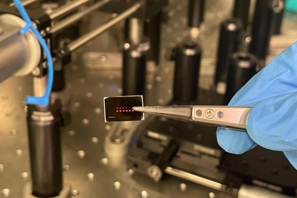
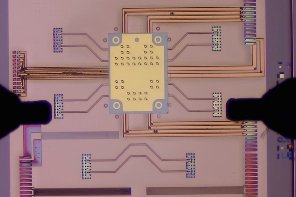
Fabricated VCSEL devices at ICS, Manchester
The hefty price tag on Quantum 2.0
Product pricing depends heavily on manufacturing yields. For VCSELs for consumer applications, 200,000 devices can come from a 150 mm wafer, with typically yield resulting in a cost of around $2-3 per laser. That’s not a feasible price-point for highly customised VCSELs for quantum applications.
VCSELs can also serve in other alkali metal vapour-based quantum systems, such as quantum magnetometers and gyroscopes, where they are again used for coherent population trapping. In all these products, other custom components are also required, such as: wafer cells to contain the alkali metal species; niche optics; crystal oscillators, in the case of atomic clocks; and shielding and/or coils, when fabricating gyroscopes and magnetometers.
Progress is being made on all these fronts. For example, MEMS wafer cell technologies are emerging. However, in addition to efforts at improving yield, a lot of fundamental research and development still needs to be undertaken to understand the effect of process and cell parameters on application performance.
One crucial question plaguing the quantum sector is this: What level of product mark-up is tolerable for end-users, so they don’t stick to other, perhaps more proven technologies? And related to this is the question of what is the price-point at which the advantage of Quantum 2.0 is too expensive to justify? It’s an unspoken reality that quantum systems will not be widely deployed until critical components are manufactured at accessible costs, unless value at the system level far outweighs the cost. You’ll not be surprised to hear that defence and security is often the early adopter for emerging technologies, enabling low-volume production that provides a pipe cleaner step for a subsequent volume ramp.
Optical spectra of a single mode VCSEL fabricated at ICS, Manchester
Upscaling an existing asset base
The issue of manufacturability for quantum is not limited to VCSELs. There are applications requiring single-photon light sources or detectors. Producing these devices is even more challenging than VCSELs, because they are at a lower technology readiness level, having not benefited from years of volume production for non-quantum applications. Viewed in that light, it’s not that surprising that miniaturised atomic clocks are one of the first quantum systems to be commercialised.
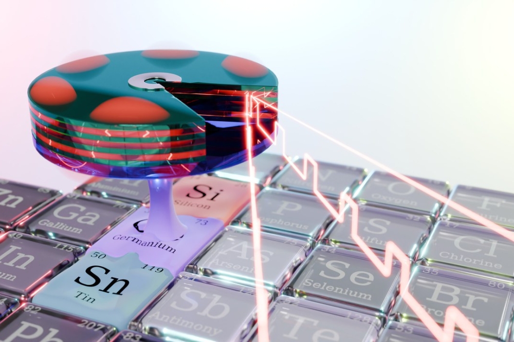
The lack of maturity in the production of some types of devices, along with their high manufacturing costs, creates a substantial barrier for many quantum industries, including quantum key distribution, quantum sensing and quantum computing. The solution is to manufacture quantum devices alongside other semiconductor processes, and leverage existing assets and infrastructure.
Helping to bridge that gap is a £5.8M project, part-funded by the UK Quantum Technologies Challenge under UK Research & Innovation (UKRI) over three years and draws on existing assets and infrastructure across 12 partners in the UK. This venture, the QFoundry project is establishing a foundry for quantum photonic components and is focused on upscaling manufacturability of these devices and understanding drivers of yield, reproducibility and reliability.
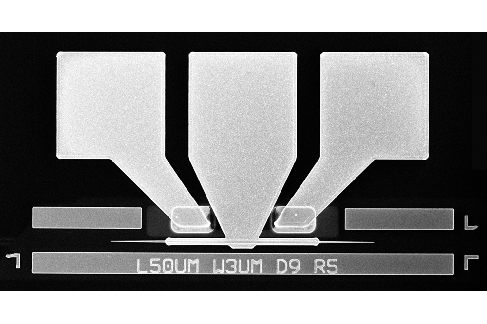
Another contributor to the progress made by CSC is through the CSconnected compound semiconductor cluster in South Wales, that is supported under UKRI Strength in Places programme and is actively involved in establishing UK supply chains for a range of quantum technologies. CSC, which has access to volume MOCVD reactors through IQE, works closely with Cardiff University who have developed a novel Quick Fabrication (QF) VCSEL process to determine impact of material design changes or growth parameters in less than half the time it would normally take to fabricate full devices.
Those that have read Move Over MOCVD (issue V, p. 20, 2022) may wonder why MBE is not the growth method of choice, given its capability to deliver superior uniformity. However, the reason is simple: MBE growth would cast an additional financial burden on the already high cost for custom design and fabrication of VCSELs for quantum technologies. To ensure the success of quantum, its devices must be made alongside volume platforms and create additional market opportunities for the same wafer platform.
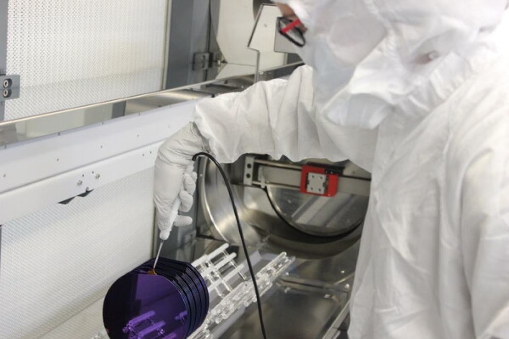
A Quick Fabrication VCSEL structure produced at Cardiff University.
Underscoring the importance of running quantum fabrication alongside standard volume semiconductor processes is the approach taken by the leading developer of quantum computers, PsiQuantum, which has partnered with Global Foundries. According to PsiQuantum, the only path to creating a commercially viable quantum computer is the one that leverages the trillions of dollars invested in the semiconductor industry, which now dates back more than half a century. Through collaboration with Global Foundries, PsiQuantum gains access to high-precision lithography and other high-end toolsets, as well as running design-of-experiments at volume to accelerate development.
It’s a sure bet that one day quantum will be a natural part of everyday life. However, getting there involves tackling fabrication challenges, and taking sensible pathways to commercialisation and eventual volume deployment.
Further Reading
Hentschel, C. et al. “Gain measurements on VCSEL material using segmented contact technique.” J. Phys. D. 56 74003 (2023)
J. Baker et al. “VCSEL quick fabrication of 894.6 nm wavelength epi‐material for miniature atomic clock applications.” IET Optoelectron. 17 24 (2022)
J. Baker et al. “VCSEL quick fabrication for assessment of large diameter epitaxial wafers.” IEEE Photonics J. 14 1530110 (2022)


