+44 (0)24 7671 8970
More publications     •     Advertise with us     •     Contact us
 
Loading...
News Article

Advanced Micro Foundry and Ascenta Technologies launch MPW runs

News

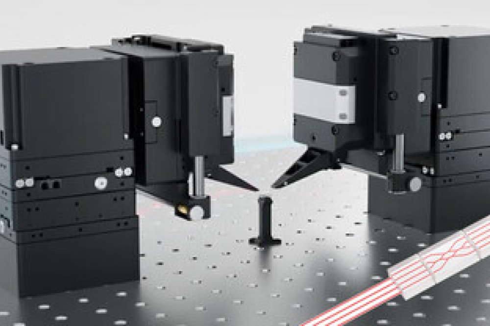
Advanced Micro Foundry (AMF) and Ascenta Technologies (Ascenta) have announced a new milestone in their collaboration: The AMF Visible + Infrared (IR) multi-project wafer (MPW) series. AMF is a Silicon Photonics foundry, while Ascenta is a spin-off led by researchers from the Max Planck Institute of Microstructure Physics and the University of Toronto. With this project, the two companies aim to bring a versatile and functional Visible + IR platform to the photonics community.

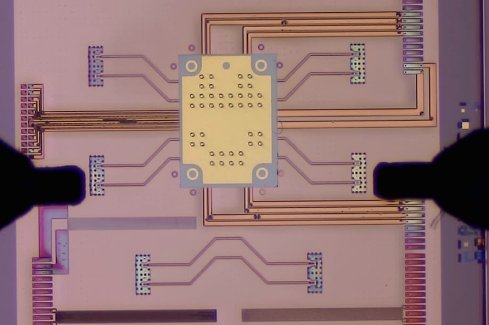
The visible platform was built using AMF’s expertise in low-loss SiN platform technology, leveraging a multi-layer silicon nitride and silicon stack. AMF says that this platform enables the creation of high-and low-confinement single-mode waveguides, effectively spanning a wavelength spectrum of 400 nm to 1600 nm, as well as active functionalities including photodetectors and highly efficient phase shifters.

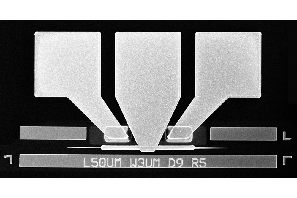
AMF partnered with Ascenta to develop a library of Visible and IR photonic components on AMF’s silicon nitride technology platform. The library includes a suite of devices such as low-loss waveguides, fiber-to-chip couplers, photodetectors, thermo-optic phase shifters, MEMS structures, and modulators. This collaborative offering seeks to empower optical designers with the necessary tools to design complex PICs with confidence, paving the way for further innovation.

Both companies are actively aggregating users for MPW runs in 2024. The AMF Visible MPW offering aims to advance visible product development in fields ranging from LiDAR, optical computing, health, and augmented reality.

AMF CTO, Dr. Patrick Lo remarked “I am very excited to see the interest from the community to utilise the wide space of visible applications. AMF is very proud to partner with Prof. Joyce Poon & Ascenta to provide access to this platform via MPW to support the community and grow the market”.

Ascenta CEO, Mr. Ilan Almog added “The Ascenta team is grateful for our partnership with AMF and thrilled to share the VIS+IR silicon photonics platform with MPW participants. The platform is the same fundamental technology Ascenta is using to develop its products, in the 3D sensing space and beyond. We are excited to enable the wide range of applications brought forth by the creativity of the community, leveraging the capabilities in the platform”.

Samco Inc announces sale of etching systems to III-V Lab
European Innovation Council funds QuiX Quantum
Intel and Source Photonics partner on 800G transceivers
LioniX secures €1.5 million in bridge financing
A technique for 3D nanostructuring inside silicon
Senergetics wins Gerard and Anton Award
Scantinel announces new CMOS-based LiDAR chip
Project to miniaturise spectrograph wins €3.4 million
EU invests €325 million in Europe's semiconductor ecosystem
Fraunhofer IPMS developing near-infrared silicon-based photodiodes
PhotonDelta opens US office in Silicon Valley
EU funds integrated photonics for space navigation
Maryland Department of Commerce funds PIC testing and packaging facility
Lightmatter appoints Simona Jankowski as chief financial officer
scia Systems to showcase ion beam processing advances at SEMICON West
Quantifi Photonics announces Iannick Monfils as new CEO
Nokia and TTI achieve 800G on long-haul commercial network
Nokia to acquire Infinera for $2.3 billion
Advancing AI with programmable silicon photonics
Quantum PICs: Empowering designers with accurate simulations
Enabling efficient light emission and detection
Harnessing InP for applications beyond optical communications
POET wins “Best Optical AI Solution” in AI Breakthrough Awards
Intel reveals fully integrated optical I/O chiplet
People, planet, profits: a sustainable way forward for all
A bright future for the global PIC market
Atom-thin silicon-germanium sheets for integrated photonics
BAE Systems and GlobalFoundries partner on semiconductors
Wave Photonics raises £4.5 million in seed funding
Aeva to supply LiDAR for AutomatedTrain project in Germany
Black Semiconductor raises €254.4 million for graphene chips
Pooya Tadayon joins Ayar Labs

×
Search the news archive

To close this popup you can press escape or click the close icon.
Logo
×
  • 1st January 1970
  • 1st January 1970
  • 1st January 1970
  • 1st January 1970
  • 1st January 1970
  • 1st January 1970
  • 1st January 1970
  • 1st January 1970
  • View all news 22645 more articles
Logo
×
Register - Step 1

You may choose to subscribe to the PIC Magazine, the PIC Newsletter, or both. You may also request additional information if required, before submitting your application.


Please subscribe me to:


You chose the industry type of "Other"

Please enter the industry that you work in: