
Sandia Labs announces method to integrate microscale optical devices on silicon microchips
Sandia National Laboratories has been awarded a patent for developing a novel method of integrating microscale optical devices onto silicon. Using this technique, the R&D centre, which is based in Albuquerque, New Mexico, created a microscale laser embedded in silicon. While similar lasers have been built before, the company says this is the first time that such a device could function within photonic integrated circuits. This technology could be applied to make self-driving cars safer, data centers more efficient, biochemical sensors more portable and radars and other defense technologies more versatile.
While silicon is the mainstay of the semiconductor and computer chip industries, it is not a good material for making lasers. This poses challenges for the development of microscale optical devices for use in these technologies. One approach to tackling this obstacle is to design a way for optical components made from a variety of materials to coexist on a silicon microchip.
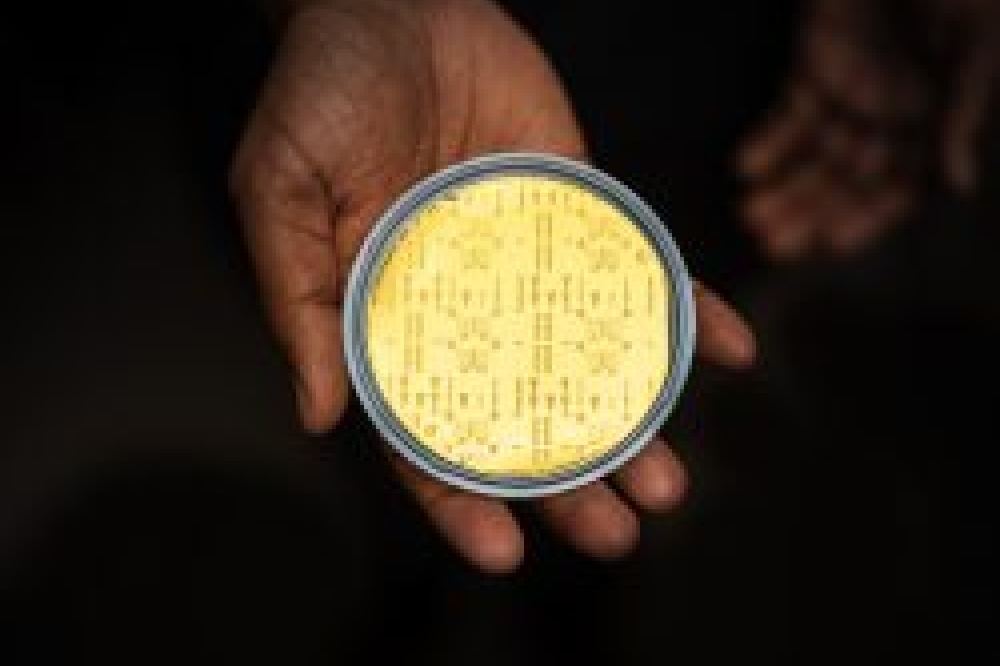
However, these kinds of materials can’t just be glued into place. Instead, Sandia research scientist Ashok Kodigala, a co-inventor of the new technique, fused them to silicon in complex layers, a process also called heterogeneous integration.
The Sandia team successfully demonstrated heterogenous integration techniques to create hybrid silicon devices: hybrid lasers and amplifiers made from both indium phosphide and silicon, and similarly modulators made of both lithium-niobate and silicon, which encode information in light generated from the lasers. Moreover, high-power and high-speed germanium detectors were developed to keep up with the lasers and modulators under the same platform.
With this method, Sandia can build many critical components for high-power optical systems, including high-bandwidth, high-speed optical devices, such as indium phosphide lasers, lithium niobate modulators, germanium detectors and low-loss acousto-optic isolators.
Other organizations, including the University of California, Santa Barbara, and Intel Corp., have built similar lasers, but Sandia has broadened the class of devices that can be integrated. For the first time, these devices could work together on optical microchips, also called photonic integrated circuits.
Semiconductor fabs could use Sandia technique/US leadership
Sandia built its chip-scale lasers with a goal of transferring the technology to industry, and stated that the achievement could strengthen America’s leadership in semiconductor technology. The team used many of the same tools found at commercial semiconductor plants, and the lasers generate light in wavelengths commonly used in the telecommunications industry, called the C-band and the O-band.
“Once we demonstrate this photonic platform at a national lab, we can then pass this technology to U.S. companies, where they can focus on even larger-scale production for commercial and U.S. government applications,” Kodigala said.
“This allows the U.S. to lead and have less dependency on foreign manufacturing capabilities,” said Patrick Chu, who co-leads the National Security Photonics Center, a group of more than 60 photonics scientists and engineers at Sandia’s
Microsystems Engineering, Science and Applications complex.
The new technique was conceived with funding from Sandia’s Laboratory Directed Research and Development program and developed it under a Defense Advanced Research Projects Agency program called Lasers for Universal Microscale Optical Systems.
Photonic semiconductors support CHIPS and Science Act
President Biden made headlines in 2022 when he signed the CHIPS and Science Act, a nonpartisan, $52.7 billion boost for the semiconductor industry. While the legislation is expected to increase production of American-made computer chips, it also directs funding for photonic semiconductors.
Sandia is also investing in optical microchips because they transmit more information than conventional ones. But manufacturing challenges have prevented their widespread adoption, Chu said. Even though the technology is well known in scientific circles, on most microchips, he said, electronic technologies still reign supreme.
With a working platform to build photonic circuits, Sandia has positioned itself to support industry and other institutions performing photonics research and development in the coming years. Sandia research is not currently funded by the CHIPS Act.
“We know our process is scalable, so that’s one way we’re supporting the CHIPS Act mission,” Chu said. “Sandia is eager to collaborate with others and start building new technologies together.”


