
NTT achieves 300 GHz band transmission with beamforming
Establishes foundation for instantaneous transmission of ultra-high-capacity data to mobile devices
NTT and researchers at the Tokyo Institute of Technology have successfully demonstrated a phased-array transmitter module to enable instantaneous ultra-high capacity data transmission to mobile receivers.
The compact four-element phased-array transmitter module uses CMOS and InP chips on the same printed circuit board. With a steering range of 36 degrees, maximum data rate of 30 Gbps, and communication distance of 50 cm, this transmitter module has succeeded in achieving the world’s first high-speed wireless data transmission in the 300 GHz band using beamforming.
The details were revealed at the 2023 IEEE MTT-S International Microwave Symposium (IMS2023), held in San Diego, Calif. in June 2023.
The 300 GHz band is expected to be used for 6G wireless communications systems. While the band has the advantage of being able to use a wide frequency range, it faces the problem of large path loss during signal propagation through space. Beamforming technology, which concentrates and directs radio energy toward the receiving device, can overcome this problem.
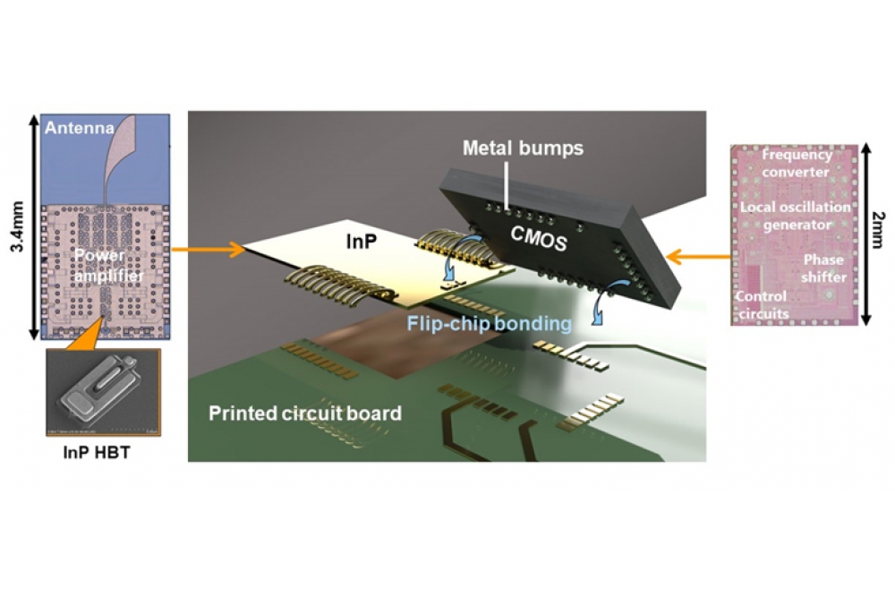
The InP chips, built using NTT's InP-based heterojunction bipolar transistor (InP HBT) technology, integrate the company's high-output power amplifier circuit and antenna circuit. Tokyo Tech developed the CMOS chip containing the frequency conversion and control circuits.
For the power amplifier circuit, high output power is achieved by combining electrical power output from multiple amplifier elements using a low-loss power combiner. The circuit amplifies the signals output from the CMOS chip and radiates the radio wave to the receiving device from the antenna packaged on the same chip.
Conventionally, to connect different types of ICs for the 300 GHz band, each IC is mounted on a waveguide module, and the modules are connected together. However, this approach has the problem of energy loss when radio waves pass through the waveguides. NTT and Tokyo Tech solved this problem through flip-chip bonding of the CMOS and the InP chips and connecting them using metal bumps of several ten micrometers in size. This packaging approach reduces connection loss and achieves high-output power .
Future Research
Short-distance mobile communication devices are expected to be deployed in 6G networks in the future. NTT and Tokyo Tech’s developed technology promises to expand these applications, such as interactive kiosks and femtocells.
The developed technology demonstrated one-dimensional beamforming. NTT and Tokyo Tech are now working on demonstrating two-dimensional beamforming with a 2D array and extending the communication distance by increasing the number of arrays. NTT and Tokyo Tech are also engaged in the development of receiver modules to meet the needs of 6G applications, and in the practical implementation of wireless communication with transmission capacity ten-fold greater than is available today.


