
MIT team grows arrays of perovskite nanoLEDs
New technique produces perovskite nanocrystals right where they’re needed
Halide perovskites are attracting attention for their optoelectronic properties and potential applications in devices such as high-performance solar cells, LEDs, and lasers.
So far these materials have mainly been implemented into thin-film or micron-sized device applications. But precisely integrating them at the nanoscale could allow on-chip light sources, photodetectors, and memristors.
Achieving this integration has remained challenging because this delicate material can be damaged by conventional fabrication and patterning techniques. To overcome this hurdle, MIT researchers created a technique that allows individual halide perovskite nanocrystals to be grown on-site where needed with precise control over location, to within less than 50 nanometers.
The paper 'On-site growth of perovskite nanocrystal arrays for integrated nanodevices' is published in Nature Communications.
They say that the size of the nanocrystals can also be precisely controlled through this technique, which is important because size affects their characteristics. Since the material is grown locally with the desired features, conventional lithographic patterning steps that could introduce damage are not needed.
The technique is also scalable, versatile, and compatible with conventional fabrication steps, so it can enable the nanocrystals to be integrated into functional nanoscale devices. The researchers used this to fabricate arrays of nanoLEDs with potential applications in optical communication and computing, lensless microscopes, new types of quantum light sources, and high-density, high-resolution displays for augmented and virtual reality.
“By moving past the traditional boundaries of nanofabrication, materials engineering, and device design, these techniques can allow us to manipulate matter at the extreme nanoscale dimensions, helping us realize unconventional device platforms important to addressing emerging technological needs,” says Farnaz Niroui, an assistant professor of Electrical Engineering and Computer Science (EECS), a member of the Research Laboratory of Electronics (RLE), and senior author of a new paper describing the work.
Tiny crystals, huge challenges
Integrating halide perovskites into on-chip nanoscale devices is extremely difficult using conventional nanoscale fabrication techniques. In one approach, a thin film of fragile perovskites may be patterned using lithographic processes, which require solvents that may damage the material. In another approach, smaller crystals are first formed in solution and then picked and placed from solution in the desired pattern.
“In both cases there is a lack of control, resolution, and integration capability, which limits how the material can be extended to nanodevices,” Niroui says.
Instead, she and her team developed an approach to 'grow' halide perovskite crystals in precise locations directly onto the desired surface where the nanodevice will then be fabricated.
Core to their process is to localise the solution that is used in the nanocrystal growth. To do so, they create a nanoscale template with small wells that contain the chemical process through which crystals grow. They modify the surface of the template and the inside of the wells, controlling a property known as “wettability” so a solution containing perovskite material won’t pool on the template surface and will be confined inside the wells.
“Now, you have these very small and deterministic reactors within which the material can grow,” she says.
And that is exactly what happens. They apply a solution containing halide perovskite growth material to the template and, as the solvent evaporates, the material grows and forms a tiny crystal in each well.
A versatile and tunable technique
The researchers found that the shape of the wells plays a critical role in controlling the nanocrystal positioning. If square wells are used, due to the influence of nanoscale forces, the crystals have an equal chance of being placed in each of the well’s four corners. For some applications, that might be good enough, but for others, it is necessary to have a higher precision in the nanocrystal placement.
By changing the shape of the well, the researchers were able to engineer these nanoscale forces in such a way that a crystal is preferentially placed in the desired location.
As the solvent evaporates inside the well, the nanocrystal experiences a pressure gradient that creates a directional force, with the exact direction being determined using the well’s asymmetric shape.
“This allows us to have very high precision, not only in growth, but also in the placement of these nanocrystals,” Niroui says.
They also found they could control the size of the crystal that forms inside a well. Changing the size of the wells to allow more or less growth solution inside generates larger or smaller crystals.
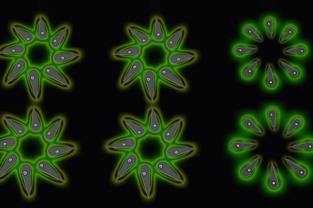
They demonstrated the effectiveness of their technique by fabricating precise arrays of nanoLEDs. In this approach, each nanocrystal is made into a nanopixel which emits light. These high-density nanoLED arrays could be used for on-chip optical communication and computing, quantum light sources, microscopy, and high-resolution displays for augmented and virtual reality applications.
In the future, the researchers want to explore more potential applications for these tiny light sources. They also want to test the limits of how small these devices can be, and work to effectively incorporate them into quantum systems. Beyond nanoscale light sources, the process also opens up other opportunities for developing halide perovskite-based on-chip nanodevices.
This work was supported, in part, by the National Science Foundation and the MIT Center for Quantum Engineering.


