
X-Fab leads EU-funded photonics consortium
photonixFAB project aims to industrialise the European silicon photonics value chain
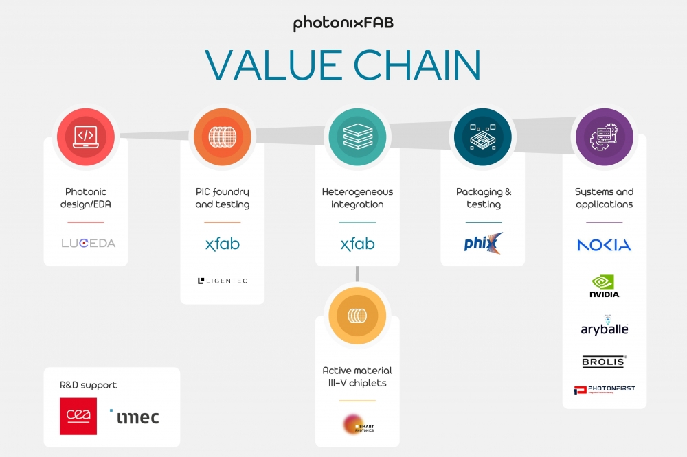
X-Fab is spearheading an initiative to enable the European semiconductor and photonics industries to gain greater sovereignty. The photonixFAB project aims to empower photonics innovation by providing low barrier access to both low-loss silicon nitride (SiN) and silicon-on-insulator (SOI) based photonics platforms with InP and lithium niobate (LNO) heterogenous integration capabilities.
The photonixFAB consortium is made up of public and private enterprises, plus research institutes – all focusing on the development and production of next-generation silicon photonics. They include LIGENTEC, SMART Photonics, PHIX Photonics Assembly and Luceda Photonics plus application developers Nokia, NVIDIA, Aryballe, Brolis Sensor Technology and PhotonFirst, as well as the major research organisations CEA-Leti and IMEC.
The objective is to establish a European photonics device value chain and initial industrial manufacturing capabilities. Thus, providing a path to scalable high-volume manufacturing for innovative product developers.
A comprehensive set of photonics foundry and assembly capabilities will be covered by photonixFAB. These will include:
• Industry-scale silicon photonics manufacturing services with low entry barriers and fast turnaround times for both low-loss SiN and SOI based PICs.
• Enablement of microtransfer printing and direct bonding technologies for InP, LNO and germanium based active and passive component heterogeneous integration on SiN and SOI based PIC platforms.
• Development of scalable packaging and testing solutions in alignment with the (heterogeneous) PIC platform developments.
• Process design kit based design automation enablement for the photonic platforms.
As a part of the project, six demonstrators are being built to validate the implemented photonics value chains. These include applications such as datacom and optical switches, coherent optical transceiver, IR spectrometer for sensing, digital olfaction sensor for consumer healthcare and a health monitoring demonstrator.
Prospective opportunities for the cutting-edge photonic devices fabricated via the photonixFAB project have already been identified. Among them are data communication, telecoms, biomedical sensors/detectors, quantum computing and vehicle LiDAR.
“Seeing huge potential emerging there, traditional semiconductor vendors, OEMs and start-ups are all now exploring photonic-enabled applications,” states Rudi De Winter, CEO of X-Fab. “Consequently, this is the right time for companies to work together on building an extensive Europe-centric silicon photonics ecosystem that will help drive the continent’s competitiveness in this exciting new market.”
The project is being supported by the Key Digital Technologies Joint Undertaking (KDT JU), with funding from EU and the national authorities. The combination of this funding and the investments being directly made by each of the consortium members comes to a total of €47.6 million. A major part of the work of this 3.5 year project will be conducted at X-Fab’s foundry operation in Corbeil-Essonnes, France, with additional activities also undertaken at the numerous other partners’ sites across Europe.


