Getting photonic crystal nano-lasers on silicon
Recent demonstrations of photonic crystal lasers on a silicon platform highlight the tremendous potential of these devices for providing efficient light sources for silicon nanophotonic integrated circuits.
BY MINGCHU TANG FROM UNIVERSITY COLLEGE LONDON
Semiconductor lasers have come an awfully long way since they emerged from a number of industrial labs in the US in 1962. To realise lasing in those first homostructure devices, the chips would be cooled by liquid nitrogen and electrically pumped with incredibly short, high-current pulses. Fortunately, rapid progress followed the invention of this device, with the introduction of double heterostructures and refinements to the active region improving key characteristics and enabling the production of a practical device.
These advances have spurred the commercialisation of the semiconductor laser and its widespread deployment. Significant successes include miniature sources for reading optical discs, the key technology for CD and DVD players, and the manufacture of countless light engines for various optical networks that underpin communication and the internet.
Now there is much interest in using III-V lasers for silicon photonics. Producing integrated circuits that route light through waveguides and a number of on-chip devices enables energy savings in many different applications requiring data transfer, such as high-performance computing and data centres, as well as opening up many new markets, including those in healthcare, where miniaturisation is highly valued.
A significant challenge with any silicon photonic integrated circuit is how to incorporate the III-V laser onto the chip. One option is bonding, using the likes of benzocyclobutene (BCB) or oxygen atoms to form a bonding interface. Intel has successfully commercialised this integration method, employing it for the production of silicon optical transceivers operating at 100 Gbit/s. However, the price of these components is at odds with the needs of silicon photonics, which requires a low-cost, high-yield, CMOS-compatible optical communication platform.
A more attractive alternative for bringing laser light to the silicon photonic chip is direct epitaxy. MBE and MOCVD have been used to grow III-Vs on silicon platforms. Recently, this has been shown to be an efficient way to fabricate silicon-based III-V lasers, due to the merits of low cost and large scale. However, despite significant demonstration of conventional Fabry-Pérot and distributed feedback lasers on III-V and silicon platforms, there is still the need for microscale and nanoscale laser devices with far lower energy consumption and optical mode control for silicon-based nanophotonic integrated circuits. Such circuits are promising candidates for next-generation quantum computing and optical microprocessors, and could be used to make microelectronic components for optical/photonic microprocessors.
Helping to lay the foundations for the development of miniature laser sources are the microdisk lasers, a triumph of the 1990s. At the heart of these devices are micro-resonators, a few micrometres in diameter. These structures support whispering-gallery modes, instrumental to single-mode lasing and low operating powers.
Photonic crystal cavities
Building on this concept – and shrinking the footprint of the laser while maintaining its excellent performance – are designs employing a photonic crystal cavity. Thanks to an enhanced light-matter interaction within the photonic cavity, the photonic crystal laser not only benefits from a smaller footprint that is nanoscale in size, but strong optical confinement that comes from the designed photonic bandgap (the primary strengths of the photonic crystal laser, compared with its edge-emitting variant, are listed in Table 1).
Table 1. Comparison of the edge-emitting laser and the photonic crystal laser.
One option for integrating a photonic crystal laser with a silicon platform is to bond the light source to a silicon or silicon-on-insulator substrate. Several groups have done just that, including those at the University of Tokyo and the University of Paris-Saclay (see Figure 1 (a)). The greatest advantage of this technique is that it has the potential to couple laser emission to a waveguide, thereby creating a platform for nanophotonic integrated circuits along with other photonic components. However, yields can be very low, hampered by ultra-high requirements for alignment – a challenge that is magnified with micro and nanoscale fabrication.
Figure 1. Two different integration methods for photonic crystal lasers on silicon: (a) bonding a III-V nanobeam laser on silicon-on-insulator substrate via BCB material; (b) and direct growth of a III-V photonic crystal laser on a silicon substrate.
Our team at UCL is pioneering a more straight-forward approach to fabricating silicon-based photonic crystal lasers, based on the use of direct epitaxy to deposit high-quality III-V materials on silicon (see Figure 1 (b)). This method promises to enable the simultaneous fabrication of many photonic crystal lasers, which significantly increases yield and makes massive production possible.
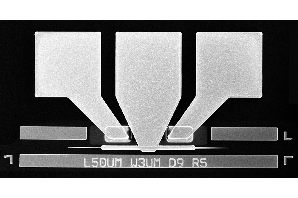
We have demonstrated the feasibility of massive production of photonic crystal lasers on silicon with our direct growth method by fabricating a nanobeam (one-dimensional photonic crystal) laser array (see Figure 2). Working in partnership with scientists from the Chinese University of Hong Kong and Grenoble Alpes University, we have broken new ground by developing the first III-V two-dimensional and one-dimensional photonic crystal lasers that are directly grown on silicon substrates.
Growing on silicon
It is far from easy to grow high-quality III-V layers on silicon. Barriers to success include dissimilarities in material properties, such as differences in lattice constant, polarity and thermal expansion coefficient. These differences give rise to a high density of crystal defects, which trap numerous carriers, causing additional heating to the chip. Thus, it is crucial to epitaxially grow high-quality III-V materials on a silicon platform, because this is key to realising high-performance III-V lasers on silicon. We have excelled in this regard, growing III-V materials on silicon that have a crystal quality that is very close to that of the III-V native substrate.
To ensure high-crystal-quality III-V materials on silicon, we use a specially designed epitaxial buffer layer to prevent: a one-dimensional defect, namely threading dislocations; and a two-dimensional defect, antiphase boundaries. Working with our collaborators at Grenoble Alpes University, we have employed MOCVD to create double silicon atomic steps on the silicon (100) on-axis substrate to avoid formation of antiphase boundaries. The two-dimensional defects, antiphase boundaries, degrade device performance by splitting materials into different domains.
There’s a need for this innovation, because prior to treatment, the silicon on-axis (001) surface is covered by single atomic steps. These single steps are to blame for forming antiphase boundaries, which arise when polar III-V materials are directly grown on the non-polar silicon surface.
By switching to a double atomic step, we avoid the formation of antiphase boundary. Evidence of this is provided by the use of hydrogen atoms to destroy the atomic bond between Si-Si atoms under high temperature. Thanks to these double atomic steps, we have grown on silicon a III-V, GaAs, that is free from antiphase boundary defects and has low roughness. Our approach has been widely used with 300 mm silicon substrates, highlighting its potential to slash fabrication costs compared with growth on III-V substrates, as well as the promise of processing our material with state-of-art CMOS fabrication equipment.
Another challenge of growing III-Vs on silicon is accommodating the large lattice mismatch that threatens to introduce a high density of threading dislocations – they could be in the region of 1010 cm-2 at the interface of III-Vs and silicon.
The mismatch is significant: there’s a difference of 4 percent between GaAs and silicon, and 7 percent between InP and silicon. Part of the solution is to introduce strained-layer superlattices, which have repeated layers of both tensile and compressive strain. When this is added, threading dislocation density fall to a practicable level for making a device of less than 107 cm-2. This is realised by pushing and pulling the propagation of threading dislocations into the horizontal direction, so they no longer impact the gain materials grown on top.
Additional improvement comes from a high-temperature annealing process, which encourages threading dislocations to move, encounter one another and merge. When annealing is combined with strained-layer superlattices and double atomic steps on silicon, the epitaxial quality of our photonic crystal lasers that are grown on silicon is comparable to heterostructures formed on native III-V substrates.
As well as a high crystal quality, our photonic-crystal lasers need a suitable active region. Over many years, quantum wells have provided gain material in various types of laser, due to their high output power and tremendous optical gain. But they are not ideal in our case, because residual threading dislocations are present in III-V materials grown on a silicon platform, even after careful design of the III-V buffer layer – and as the device operates, the number of threading dislocations grow, degrading device performance. The long-term impact is significant, including diminished output power, a shortened device lifetime and a hike in temperature instability.
Figure 2. A scanning electron microscope image of a fabricated one-dimensional photonic crystal laser array.
Drawing on dots
We have found that a far better alternative for providing gain is the self-assembled quantum dot. When dots are deployed in the active region, they have a high tolerance to threading dislocations – this could lead to threading dislocations forming closed loops, which reduce the extent of device degradation.
Employing the techniques mentioned above, we have produced optically pumped III-V quantum dot lasers on silicon that feature a photonic crystal cavity. These nanobeam lasers have many promising characteristics, including: an ultra-low threshold, with a pumping power below 1 µW; a nanoscale footprint of around 8 µm by 0.53 µm by 0.36 µm, for a one-dimensional photonic crystal cavity; and a high-temperature performance, exceeding 60 °C. These characteristics show that our nanobeam lasers could serve in silicon-based nanophotonic integrated circuits.
Our next challenge is to realise electrical operation with our photonic-crystal laser on a silicon platform. This can be accomplished by using ion implantation to introduce different n-type and p-type contact layers on the planar photonic crystal cavity.
Figure 3. A nanobeam laser directly grown on silicon substrate with a nanoscale footprint and ultra-low threshold.
It is worth noting that we have the opportunity to turn to some advance types of photonic-crystal cavity. They include the photonic crystal surface emitting laser (PCSEL), which combines the VCSEL’s advantages of round beam shape and a high output power of more than 1 W with the high speed and low cost of the edge-emitting laser. Compared with the VCSEL, the PCSEL offers a simpler fabrication process, by using a photonic-crystal cavity to confine light horizontally. This approach avoids the process of oxidation in confining layers.
Another drawback of the VCSEL is that it requires a very high thickness of DBR, so growth of this class of laser on silicon would lead to a large volume of micro cracks, due to incompatible thermal expansion coefficients for the III-Vs and silicon. Turning to PCSELs-on-silicon would offer us a solution for realising high performance III-V surface-emitting lasers on a silicon platform.
When making any semiconductor laser, there are imperfections associated with light scattering at the non-smooth surface. This issue is more severe when using a nanofabrication process, and increases the difficulties of fabricating photonic crystal lasers.
A promising alternative is the topological laser, inspired by the topological insulator in electronics. Topological lasers are capable of guiding light within the designed photonic crystal pattern, and can avoid light scattering associated with imperfections in nanofabrication. Recently, working with colleagues at Grenoble Alpes University and The Chinese University of Hong Kong, we have demonstrated a topological laser with a photonic crystal cavity that’s grown on the silicon substrate, thereby showing that this is a robust nanoscale light source for silicon photonics. Even though integrating the photonic crystal laser on a silicon platform is still at an the early stage, we are convinced that this source of light is destined to play a significant role in next-generation, silicon-based nanophotonic integrated circuits.
Further reading
- T. Zhou et al. “Monolithically Integrated Ultralow Threshold Topological Corner State Nanolasers on Silicon” ACS Photonics 9 3824 (2022)
- T. Zhou et al. “Single-mode photonic crystal nanobeam lasers monolithically grown on Si for dense integration” IEEE J. Sel. Top. Quantum Electron. 28 1 (2021)
- T. Zhou et al. “Continuous-wave quantum dot photonic crystal lasers grown on on-axis Si (001)” Nat. Commun. 11 977 (2020)
- G. Crosnier et al. “Hybrid indium phosphide-on-silicon nanolaser diode” Nat. Photon. 11 297 (2017)
- B. Ellis et al. “Ultralow-threshold electrically pumped quantum dot photonic-crystal nanocavity laser” Nat. Photon. 5 297 (2011)
- K. Hirose et al. “Watt-class high-power, high-beam-quality photonic-crystal lasers” Nat. Photon. 8 406 (2014)
- T. Inoue et al. “General recipe to realize photonic-crystal surface-emitting lasers with 100-W-to-1-kW single-mode operation” Nat. Commun. 13 3262 (2022)


