

Building phononic integrated circuits with GaN
The ability to guide high-frequency sound around a semiconducting chip positions GaN as a promising platform for producing compact, high-performance acoustic wave devices.
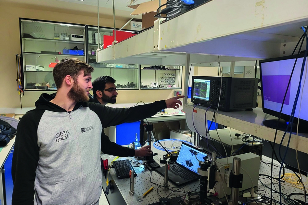
BY Mahmut Bicer, Stefano Valle, Jacob Brown, Martin Kuball and Krishna C. Balram FROM THE UNIVERSITY OF BRISTOL
A long-standing theme of engineering research is exploring and exploiting the similarities between different wave phenomena. Their similarities, such as reflection, superposition and the creation of standing waves, has been appreciated for decades, thanks in part to excellent demonstrations by the late John Shive, who worked at Bell Labs. Back in 1959 Shive gave a lucid, insightful lecture on this topic that can still be enjoyed via Youtube. In that talk, standing as one of the earliest examples of recognizing the unifying nature of the underlying physics and illustrating how to translate ideas from one field to another, Shive demonstrated his wave generator, a great contribution to teaching this topic.
One modern iteration of exploiting wave phenomena is an extension of silicon integrated photonics, with chips designed to control the propagation of sound waves with frequencies in the gigahertz domain. Such efforts build on progress in silicon photonics over the last decade that spawned a revolution in optical telecommunication, with CMOS foundries now used to build photonic chips. The underlying physics behind this development is the high refractive index contrast provided by a silicon-on-insulator platform – this enables tight confinement of propagating light in wavelength-scale waveguides. For instance, the standard waveguides used to route optical telecommunication signals with wavelengths of around 1550 nm have a cross-section of around just 220 nm by 550 nm. That’s substantial miniaturisation compared with an optical fibre: it has a typical core size of 8.2 mm and a cladding diameter of 125 mm, due to its far weaker refractive index contrast.
There are many benefits associated with the extreme confinement that enables compact devices. One great attribute is that a single chip can accommodate various passive and active functions, such as splitting signals, combining them, mode transformation modulation and detection. In addition, there is a low propagation loss that accompanies the strong confinement, resulting in high electric field strengths and associated non-linearities. These properties may be harnessed to implement a variety of functions for quantum information processing, such as single-photon generation using spontaneous four-wave mixing.
As the wavelength of sound waves in the gigahertz range is similar to that of the light used for telecommunication, it is natural to ask how far these ideas from integrated photonics can be extended to gigahertz frequency acoustic waves. One may also wonder what new device paradigms might be enabled.
It should be noted that the idea of guiding sound in waveguides is not new – this had been discussed from the very early days of waveguide research. However, this interest has evolved, and is now motivated by considerations related to the acoustic waves that underlie all the filtering in modern smartphones. Today’s state-of-the-art smartphones are packed with between 30 and 50 acoustic wave filters, with their number increasing with each successive generation. It is an ever-increasing challenge to accommodate this increasing number of discrete filters into a given area, along with the associated switches, amplifiers and other signal processing circuitry. Current devices are a packaging tour-de-force, but we cannot expect these methods to work well into the future.
The tremendous successes that have come from microelectronics, and more recently silicon photonics, indicate that monolithic integration could be the best solution to this growing problem. Success hinges on figuring out a way to trim the size of traditional acoustic wave devices, and how to implement tight integration between active and passive components on the same die. Much effort has already been directed at accomplishing this, with approaches relying on methods that employ a CMOS process to integrate existing acoustic-wave devices, such as FBAR and SAW filters, which rely on quasi plane-wave resonators. But at the University of Bristol we are taking a different path, investigating whether acoustic-wave devices can be redesigned around phononic integrated circuits (PnIC), featuring strong geometrical confinement of sound. We are keen to explore the benefits and challenges of this approach.

Figure 1. Analogy between photonics and phononics. A strong geometric index contrast leads to an increase in confinement and a reduction in the waveguide cross-section. The rise of silicon photonics is a case in point, with telecom-wavelength silicon waveguides (bottom left) having sub-micron dimensions compared with optical fibres (top left). Bringing these ideas to high-frequency acoustic waves (top right) can lead to the development of compact passive acoustic devices and the prospect of tight active-passive integration on-chip with a view towards integrated RF front-ends. The image of the FBAR Avago die is taken from R. Ruby, “A decade of FBAR success and what is needed for another successful decade,” 2011 Symposium on Piezoelectricity, Acoustic Waves and Device Applications (SPAWDA), Shenzhen, China, 2011, pp. 365-369.
Computational challenges
Another driver behind the development of PnICs, coming from a very different direction, is the rise of superconducting qubit-based quantum processors – that includes the demonstration of computational quantum supremacy by Google using this platform. A logical next step, following the development of classical information processing technologies, is the development of small quantum networks around these superconducting qubit processors.
This is challenging task, because qubits usually work in a dilution fridge environment that is just a few millikelvin above absolute zero. In addition to this temperature restriction, another issue is that the microwave quantum states cannot be sent over any significant distance, due to loss in the microwave cables.
Alternative approaches may offer a better chance of success. One promising pathway is to switch to optical photons, which have been employed in quantum communication from near-earth satellites. This scheme requires quantum transducers, which convert microwave quantum states to light and back with high efficiency. To build such a device, engineers must overcome a massive wavelength mismatch between the fields in the microwave and optical domain. Fortunately, acoustic waves provide a natural way to bridge this, having wavelengths of microns at gigahertz frequencies.
We are pursuing piezoelectric optomechanical platforms that support light and sound propagation on these wavelength scales, and foster strong acousto-optic interactions between resonant optical and mechanical modes. Such piezoelectric optomechanical devices offer one of the most promising routes towards building quantum transducers, with state-of-the-art devices achieving photon transduction efficiencies of around 5 percent.
When developing a PnIC platform, deciding on the material platform is the first and possibly the most critical choice. There’s a need for a slow-on-fast platform – in other words, a platform where the acoustic velocity in the waveguiding device layer is far lower than in the substrate – because this offers total internal reflection of sound and the prospect of waveguiding. It’s important to satisfy the guiding condition for all potential leakage modes in the substrate, and for all propagation directions simultaneously. The good news is that in practice, this condition is relatively easy to satisfy. There are a wide range of substrate velocities available in different material platforms, and many material platforms are currently being explored, ranging from lithium niobate on sapphire to GaN-on-SiC.

Figure 2. Optical microscope images of representative PnIC devices fabricated at the University of Bristol in a GaN-on-SiC platform. The acoustic waves are generated from applied RF signals using interdigitated transducers, whose fingers are curved to focus the sound into the acoustic waveguides. The waves are then routed on-chip using waveguides with cross-sectional dimensions of the order of a wavelength, and high-Q whispering gallery modes in ring resonators, which can be used for resonant devices.
Going with GaN-on-SiC
Out of the many options, which all offer unique advantages and disadvantages, we have selected GaN-on-SiC. Our primary reason for this is that GaN is a moderate piezoelectric semiconductor with a built-in foundry infrastructure that can potentially enable monolithic integration between active and passive components on the same die. By exploiting acousto-electric (electron-phonon) interactions in this platform, it is possible to develop non-reciprocal microwave devices that provide new degrees of freedom to manipulate RF signals on a chip. With alternative, existing technologies, this is only accomplished with the addition of magnetic materials.
Our PnICs feature an interdigitated transducer, which converts input microwave signals to sound waves (see Figure 2 for an optical microscope image of our device). The periodicity of our interdigitated transducer has been selected to match the acoustic (Lamb) wave frequency in the material. This ensures a periodic perturbation on the surface, due to the piezoelectric effect, and efficient conversion of microwave energy into propagating sound waves. By shaping our electrodes, we can focus sound waves efficiently into wavelength-scale waveguides that have a cross-sectional area of several square microns. Once sound is launched into these waveguides, it can be routed over the surface in an arbitrary fashion, while maintaining tight lateral confinement.
As well as producing straight waveguides, we have the opportunity to construct micro-ring resonators that exploit high-quality-factor, whispering-gallery modes of sound as the resonant building block for filters. Given that whispering-gallery modes rely on the total internal reflection of sound, which is theoretically lossless at a given frequency, resonators based on this technology should demonstrate higher quality factors than traditional SAW and FBAR devices – those incumbents rely on either metal gratings or metal contacts (hard boundaries) for reflection that’s always accompanied by excess dissipation and scattering. If we are able to experimentally verify the promise of this micro-ring resonator technology, it would show that in addition to providing compact devices, the PnIC approach can deliver devices with a higher performance than those made with traditional approaches.
The real advantage of the PnIC lies in the realisation that since sound is generated from an RF signal, its manipulation on a chip ultimately provides new degrees of freedom to manipulate RF signals. For instance, if the designer of a PnIC decides to include spiral waveguides with an on-chip footprint of less than 0.25 mm2, this allows RF signal delays of more than 2 ms, corresponding to electromagnetic delays of at least 600 m.
While our PnIC platform has shown promising initial results, there are a few important problems that we still need to address before our exciting device demonstrations can impact future RF systems. One essential area to work on is the reduction of the overall insertion loss in these platforms. Acoustic waves suffer negligible excess dissipation and scattering once inside the waveguide, but a significant insertion loss at the entrance and exit, coming from the transducer and the transducer-waveguide interface. It is a challenge to develop efficient transducers that are impedance-matched to 50 W and mode-matched to wavelength-scale waveguides.
Another issue arises because acoustic platforms are intrinsically multi-moded systems. There’s a need to carefully control mode propagation so that sound is efficiently focused into the waveguides without deleterious mode conversion at the interfaces. Note that in this instance the analogy with optics breaks down. For integrated photonics the corresponding problem is much simpler, due to both single-mode operation and the nature of the refractive index profile, which keeps light near the waveguide centre. With sound, especially surface waves, there is a preference for intensity to peak beside the edges of the waveguide.
A second thrust for our research roadmap is to push the PnIC beyond purely passive devices and exert active control on the acoustic waves propagating in these wavelength-scale devices. We would like to move towards tuneable PnICs, engineering acoustoelectric interactions in our GaN platform to provide controllable gain and non-reciprocity. Success on this front will provide new degrees of freedom to the PnIC toolkit from an RF systems perspective. Finally, it goes without saying that there’s a need to translate all these research advances to a commercial GaN foundry platform, to enable a full realisation of the system-level benefits.
We are in no doubt that by guiding and manipulating sound on the surface of a chip, wavelength-scale PnICs are providing a promising avenue to re-think passive acoustic devices from an RF systems perspective. As well as trimming the on-chip footprint, building around a waveguide geometry allows natural avenues to route and actively manipulate sound – and by extension the associated RF signal – on a chip in ways that open up new architectures for systems integration and signal processing. To realise the full benefits of this platform in the near-term there’s a need to cut insertion loss to levels comparable to current systems and produce devices with a commercial foundry process.
Further reading
- Smartphones and RF filters issues: R. Ruby “A Snapshot in Time: The Future in Filters for Cell Phones” IEEE Microwav. 16 46 (2015)
- Piezoelectric quantum transducers: K. Balram et al. “Piezoelectric Optomechanical Approaches for Efficient Quantum Microwave-to-Optical Signal Transduction: The Need for Co-Design” Adv. Quantum Technol. 5 2100095 (2022)
- Confining sound and light (mechanisms): “Controlling phonons and photons at the wavelength scale: integrated photonics meets integrated phononics“ A. Safavi-Naeinin et al. Optica 6 213 (2019)
- GaN acoustics work at Bristol: M. Bicer et al. “Gallium nitride phononic integrated circuits platform for GHz frequency acoustic wave devices” Appl. Phys. Lett 120 243502 (2022)
- Acousto-electric interactions for RF signal processing: L.Hackett et al. “Towards single-chip radiofrequency signal processing via acoustoelectric electron–phonon interactions” Nat. Commun. 12 2769 (2021)


