
On-board photonics closing the gap between PICs and glass fibers
The growing demand for higher data-rates and lower power consumption is driving the development of many photonic integrated circuit (PIC) technologies. But it is the use of on-board photonics – PCB-embedded planar waveguides - which allows getting access to the benefits of these PICs.
By Nikolaus Flöry from vario-optics ag
Photonic integrated circuits (PICs) have matured tremendously over the last decade and are being employed in a variety of use-cases nowadays. As the range of applications is expanding, more effort is put into the seamless integration of PICs within complex electro-optical modules to create all-optical system architectures. These are required to fulfill the promises of photonic systems – i.e. lower power consumption at higher bandwidth in telecom, and utilizing novel functionalities for optical sensor devices.
However, this is where most photonic chips face a big challenge: while PICs are typically tightly confined, miniaturized chips, the typical module size of a complete package includes driver electronics, fiber interfaces and other components. In the electrical world, PCBs act as the motherboard, hosting mutliple ICs and eventually being connected by wires. Analogous, in the field of photonics, Innovative solutions such as on-board optics, i.e. embedding planar waveguides made of polymer or glass material into printed circuit boards are necessary to bridge this missing gap between photonic chips and existing glass fiber networks.

The coupling loss to standard optical fibers as a function of waveguide
modefield diameter (MFD). Several PIC platforms have emerged over the
last decade, from strongly confined chips with large coupling loss to
weaker confined platforms such as polymer or glass, with good overlap to
optical fiber modefields.
Photonic Integrated Circuit Platforms
Within the last 10 years, a variety of planar waveguide platforms have been established. They differ by the used materials for the light guiding cores and surrounding cladding and respective optical properties. One of the most important material parameters is their refractive index (RI) - specifically the RI-contrast between core and cladding, as this number, among others, dictates the typical waveguides dimensions of each platform. The range spans from highly integrated silicon photonics (SiPh) or silicon nitride (SiN) platforms over lithium niobate (LiNbO) to the slightly larger glass and polymer waveguides, which exhibit dimensions similar to optical glass fibers.
For a long time, the development of most of these platforms was driven by applications from the telecommunications sector. Thus the tight integration of complex active and passive device functionalities such as AWGs and modulators at the smallest possible size on the chip level was the prime goal. SiPh as well as InP have proven to be excellent platforms for these kind of use-cases.
However, as the use of photonics is expanding the board-level, the manufacturing costs of these platforms are too high to be used for (multiple-)centimeter sized boards. Moreover, while the small waveguide cores (typically below 1 μm for SiPh or InP) have their own advantages, their associated small modefield diameters (MFDs) offer a substantial barrier when trying to couple to optical fibers.
This opens the field for less confined waveguide platforms, such as polymer or glass based photonic circuits, which can be efficiently coupled with existing optical fiber connections and manufactured at the board level.
In recent years, polymer photonics has gained tremendous attention as a result of its manufacturing simplicity. Polymer optical lenses, for example, are employed in modern smartphone cameras due to the easier fabrication, their robustness and lower costs. Similarly, polymer waveguides are an attractive alternative to other highly integrated PIC platforms such as SiPh or InP. In contrast to many other PIC platforms, polymer waveguides exhibit roughly the same dimensions and optical properties (e.g. RI) as standard optical glass fibers, which makes the combination with commonly used pigtailed laser sources or detector modules straightforward.
Similar to optical fibers, polymer waveguides can either be used in multimode (larger core dimension, typically 30 – 500 µm) or singlemode (2-5 µm core size) operation. In both cases, they are compatible with the according fiber type.
For example, the mode field diameter of singlemode optical fibers can be matched by polymer waveguides in different wavelength ranges, e.g. 4-6 µm in the visible (VIS) and 9-10 µm in the near infrared (NIR), allowing for efficient fiber-chip coupling.

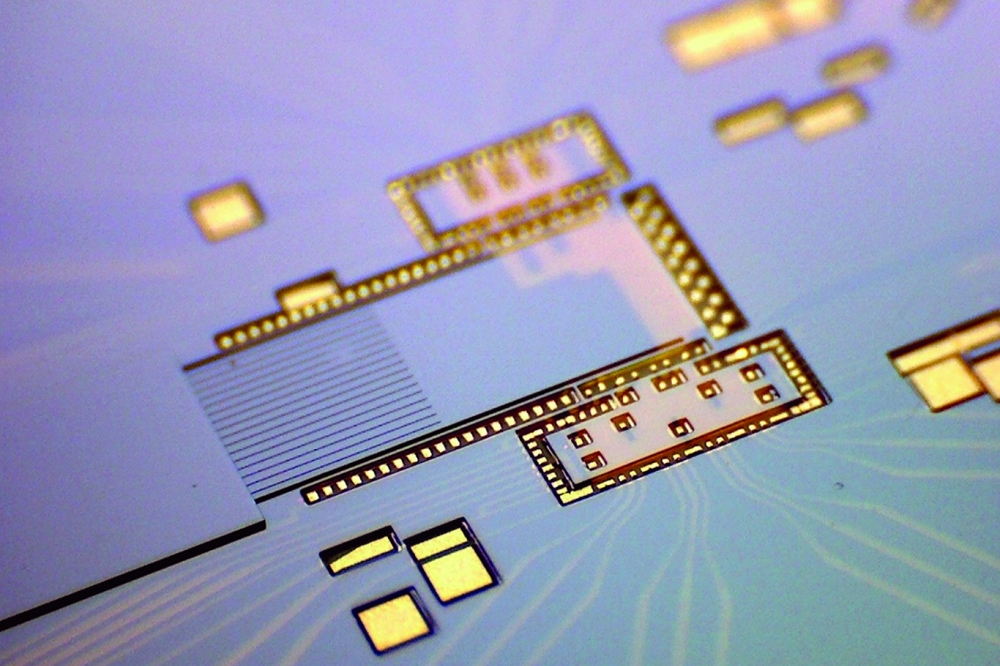
An example of an electro-optical circuit board for a sensor application.
A photonic layer is used on top of a PCB to combine light of
edge-coupled laser diodes. Such a combination of planar waveguides and
PCB technology reduces assembly efforts and enables fully integrated
electro-optical systems.
Electro-Optical circuit boards
While typical PIC chips have dimensions of just a few mm each side and are processed on fixed wafers sizes, polymer waveguides can be manufactured in sizeable quantities on large panel sizes by means of UV photolithography. Making use of the tooling and standards from the printed circuit board industry provides an easier, more common process flow, and cuts down the production costs.
This allows their employment in electro-optical circuit boards (EOCBs), which, simply put, is a board featuring both an electric interface (PCB) as well as on-board optical connections (waveguides). This renders EOCBs a prime technology platform for hybrid integration and board-level photonics. Electrical circuits on an EOCB are manufactured by standard PCB technology, allowing to include features such as high-speed RF interfaces, (glass) interposers, thermal dissipation layers and vias. Optical on-board connections are created by including polymer based planar waveguides to the board. Depending on the application, these can be either directly manufactured on-board, using the PCB or glass as a substrate.
As polymer waveguides have advanced, they can now be operated in singlemode at most common (telecommunication) wavelength and moreover provide solid environmental stability and high power thresholds. The dimensions of the cores can be freely adapted and optimized. This way, many passive in-plane device functionalities such as splitters, directional couplers or multimode-interference couplers can be realized. As a result of the rectangular cross-section, polymer waveguides are also polarization maintaining.
The possibility of having one common host board for both the electrical and optical interface is a significant advantage over other integration methods, however often not considered enough. Most PIC packaging efforts only focus on an efficient optical coupling interface. While this is of course a central motivation and requirement in a majority of use-cases, thermomechanical and electrical requirements are often hard to meet this way.
The operation of high-power laser chips and high-speed modulators, for example, make it necessary to handle the heat as well as to provide RF above > 100 GHz. EOCBs can be designed precisely for the specific equirements of a photonic application, taking into account electrical, optical and thermal considerations, before being equipped with PICs as well as purely electronic components.

Vertical coupling to embedded waveguides can be achieved using parabolic micromirror arrays, which are integrated into PCBs. This patented technology from vario-optics allows efficient coupling of e.g. VCSELS into planar waveguide routing on-board. The micromirrors can be used for collimated or focused output and are optimized for waveguide dimensions of 50 µm.

Coupling to EOCBs
Optical coupling to an EOCB can be done both in-plane or vertical out-of-plane. In-plane coupling typically relies on butt-coupling, i.e. precise facet-to-facet placement of the optical component to the waveguide core.
The efficiency of such an interface depends on the NA-match (multimode) and modefield overlap (singlemode), respectively. Thanks to the tenability of the geometry of polymer waveguide cores, their MFDs can be optimized for both coupling to a highly confined PIC, as well as to standard optical fibers. While there is the possibility to make use of precise on-board alignment features, which allow for passive placement of components, active alignment processes are becoming easier (and cheaper) over time as well and are capable to provide sub-micron assembly accuracy. An attractive alternative is vertical out-of-plane coupling. This can be achieved in multimode EOCBs by including miniaturized parabolic mirror elements into cavities inside the EOCBs. These can be positioned with high accuracy and allows to make use of VCSEL sources at very high efficiencies.
Another alternative approach to the assembly is to rely on an adiabatic, evanescent coupling interface. In this coupling scheme, inverse-tapered waveguides on the PIC are used to couple light to exposed polymer waveguide cores, and vice versa. In contrast to grating couplers, this approach provides not only relaxed lateral assembly tolerances (approximately +/- 2 µm), but also efficient coupling over a broad wavelength range for both TE and TM polarization.
Summary
On-board photonic solutions are required to utilize the full potential of integrated photonic technologies. The rise of planar waveguides based on polymer or glass is a key step towards the development of devices and applications with electro-optical functionalities, high integration density and competitive costs as compare to existing solutions. Electro-optical circuit boards, as manufactured by vario-optics ag, represent a key technological building block for such all-optical systems.
Glass-Integration into PCB
Apart from its use as an interposer, glass can also be employed as the waveguiding layer itself. Through a process based on ion-exchange, developed by Fraunhofer IZM, gradient index waveguides are created in thin glass. These embedded waveguides exhibit low-loss singlemode operation and can be manufactured on large panel sizes of up to 457 mm x 303 mm .

Together with its partner Varioprint, an advanced PCB manufacturing company, vario-optics has developed a lamination process to integrate such glass panels into electrical PCBs, similar to what can be achieved with polymer waveguides in optical backplanes.
Optical interfaces to the glass layer are made by cut-outs in the PCB and CO2 laser cutting of the glass. Laser-structuring of the panels also allows to create trough-glass vias or mechanical features for embedding optoelectronic components.Overall, due to the low propagation loss at telecommunication wavelengths (< 0.06 dB/cm @ 1550 nm , the addition of glass waveguides into large EOCBs is a promising technology for next generation photonic integration.
Reference
- Bradley Visser, et al., “Waveguide based passively demodulated photothermal interferometer for light absorption measurements of trace substances,” Appl. Opt. 62, 374-384 (2023)
- N. Flöry et al., “Highly reliable polymer waveguide platform for multi-port photonic chip-packaging,” IEEE 71st Electronic Components and Technology Conference (ECTC), 2021, pp. 1689-1694.
- L. Brusberg, M. Immonen & T. Lamprecht, “Electro- optical circuit boards with single- or multi-mode optical interconnects”, in Optical Interconnects for Data Centers, 287-307, Elsevier, 2017.
- White Paper on “Multimode Waveguide Interconnect System Design for Photonic Circuit Integration”, Consortium for On-Board Optics, 2022.
- N. Flöry, “On-Board Optics”, Feature Article in Photonics Spectra, February 2023 Issue.
- Schröder, Henning; Schwietering, Julian; Böttger, Gunnar; Zamora, Vanessa (2021): Hybrid photonic system integration using thin glass platform technology. In: J. Optical Microsystems 1 (03). DOI: 10.1117/1.JOM.1.3.033501.
- Schwietering, Julian, et al., “Integrated optical single-mode waveguide structures in thin glass for flip-chip PIC assembly and fiber coupling.”, IEEE 70th Electronic Components and Technology Conference (ECTC). 2020 pp. 148–155.


