Accelerating the photonics transition with much shorter R&D
To accelerate the transition from electronic to photonic integrated circuits (PICs), a breakthrough in cost and cycle time of the manufacturing process is needed. Etteplan developed an R&D solution which accelerates the process. The solution uses a simple and efficient block-based programming interface via a standard web browser to enable users to program the production sequences themselves.
Companies in the photonic industry, developing new products or products novelties, that are transitioning from startup to scale up and are working on the first prototypes, are seeking ways to quickly and reliably align photonic components and validate their product development. Despite all the developments, growth of integrated photonics is hampered by slow prototyping and R&D.
Technology developed in international consortium
The EU-funded ULTRAPHO project aims to validate and commercialize a novel photonics concept. It will boost Europe’s semiconductor industry to a world-leading level in the field of photonics technologies and devices that use graphene to increase the data transmission capacity of optical fibers. Goal of the ULTRAPHO FTI project is to change the market for photonic communication devices by bringing a groundbreaking technology to the market. The final goal is to establish a novel world leading enterprise in the semiconductor industry in the EU. Supported by major players like Nokia, Sony, and GlobalFoundries, the consortium members will become worldwide leaders in the emerging field of photonic technologies and devices. The fundamentally new high-speed photonic devices use graphene to increase data transmission capacity of optical fibers. Together with novel fabrication and characterization tools and technology developed and marketed by the consortium the whole value chain from fabrication to the final product is covered.
The consortium markets an ultrafast and broadband graphene photodetector which is of increasing importance for datacenters or 5G infrastructure.
A solution to accelerate photonic R&D
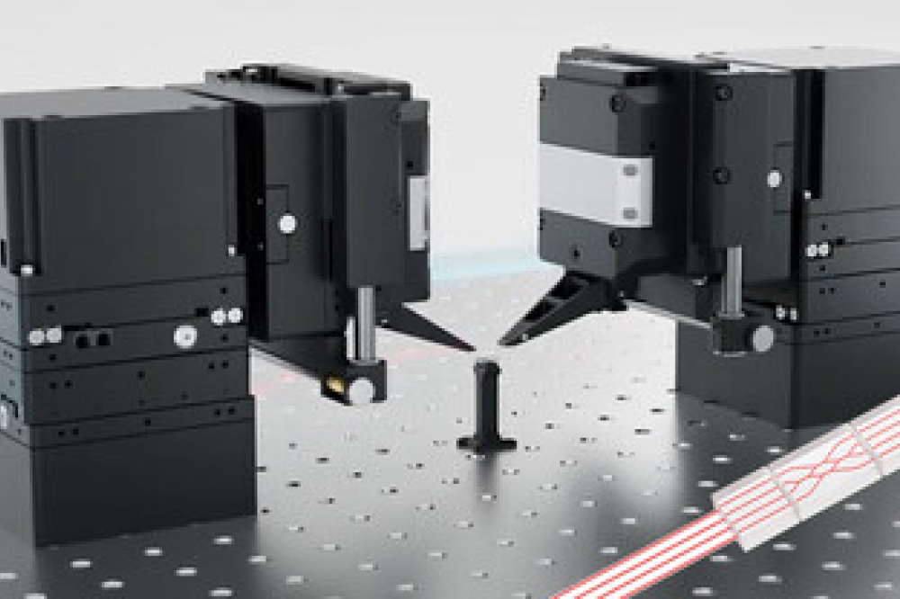
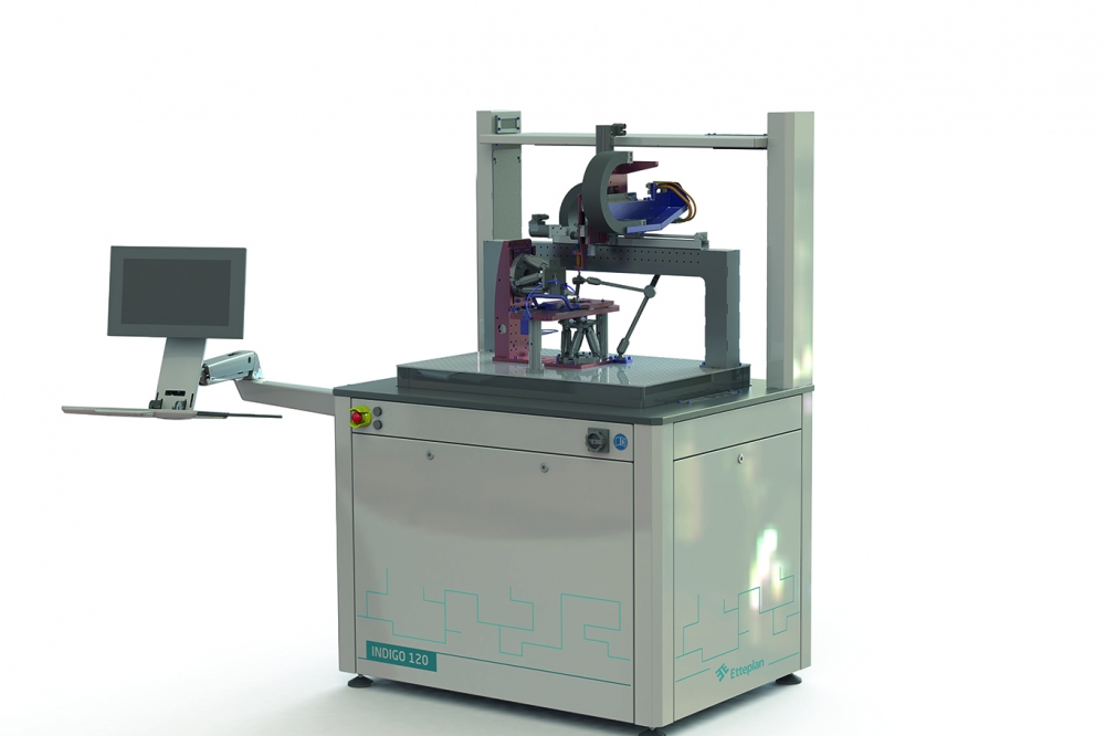
To help accelerate the photonic transition, Etteplan developed ‘Etteplan Indigo’. A modular machine platform for the assembly of a wide range of micro-optical elements, such as the graphene photodetector by Black Semiconductor and Graphenea. “Black Semiconductor and Grahenea are developing a photodector with graphene, capable of converting optical signals to RF and vice versa”, tells Niels Jansen, manager Engineering at Etteplan. “They have asked Etteplan to help find solutions for the back-end assembly of this product.
As this product was still in development, flexibility in the production sequence of the packaging solution became a crucial element. Typically it takes days of work to adjust the machine platform from product X to do a test with product Y. As a general rule, the machine supplier has to be called in to convert machine settings. If for a product change one would have to move the gantry to a different position, choose a different alignment route, this takes a lot of time with a PLC control.
You have to create it, test it offline, track software changes and someone has to come on site to adjust settings, test and validate. This quickly adds up to six to eight charged hours, provided a programmer is readily available to make these changes.
By changing production parameters or complete sequences in a simple manner, multiple variations in the product design can be tested and validated quickly and comfortably, in the end enabling the development of the product to achieve quality results and limited lead time. Etteplan developed a solution that enabled just that.
Based on the open source platform Blockly, the solution combines a simple and efficient block-based programming interface via a standard web browser to enable users to program the production sequences themselves.”
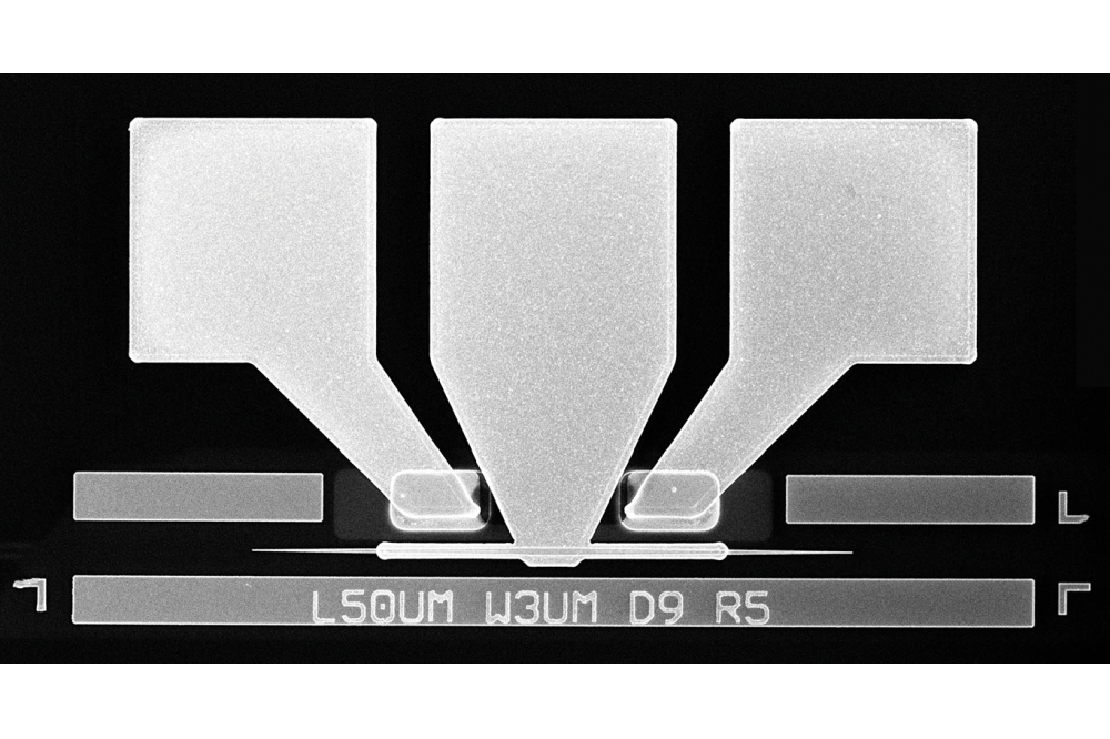
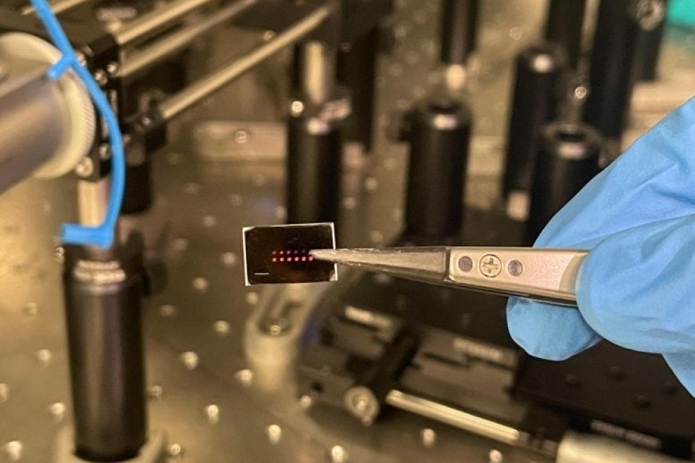
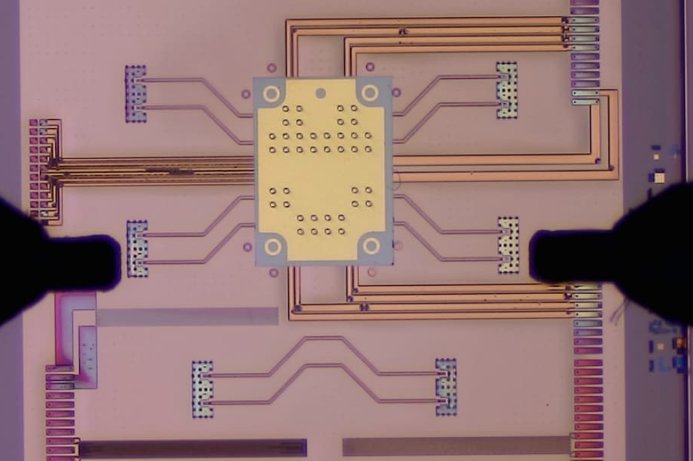
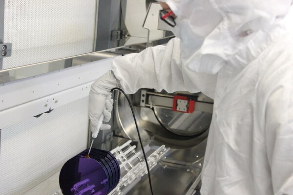
AMO’s packaged graphene photodetector. Image credit: AMO.
Make the changeover yourself
‘Etteplan Indigo’ has a short cycle time and enables a faster time-to-market for automatic and precise alignment systems, while increasing throughput tenfold with respect to currently available solutions. “But, most importantly, the flexible production solution (FPS) enables you to program the changes to package the next prototype yourself,” tells Niels Jansen, manager Engineering at Etteplan.
“Visually programmable software controls the PLC, without the need for programming by the machine manufacturer. The representation of modules in visual blocks makes it ‘child’s play’ to follow and adjust the steps in packaging. You don’t need a PhD for it so you can also quickly and easily bring relatively untrained people into production. We have taken away the complexity and dependency, and that adds a lot of speed.”
Etteplan’s Flexible production solution (FPS), visually programmable software controlling the PLC.
Etteplan’s visually programmable software.
“Our modular machine is also financially attractive in terms of investment and the machine has a smaller footprint,” states Niels Jansen. “There are no three or four machines next to each other working on different products. There is only one machine. Moreover, the reproducibility of the configured, programmed run is a big plus. The system allows you to store the programmed production sequence and configured parameters for retrieval and reuse at a later date. We therefore dare to call ‘Etteplan Indigo’ a ‘photonic breakthrough’ for good reason.”
Another benefit: shorter changeover times in higher production volumes
The machine platform meets the specific needs for usage in R&D (start-up) and scale-ups environments, enabling accurate assembly of optical elements at relative low investment cost.
“If your production volume increases, you can reconfigure the system by simply adding modules to create a fully automated assembly solution”, tells Niels Jansen. “The modular approach allows for a machine that is customized to your current demands while leaving plenty of room for the customization of different components and upgrades, and to integrate the machine into an assembly line.”
“Besides the benefit for R&D and scale-ups of faster changeovers, we also see companies with a great need for quick and easy changeover of the packaging machine in order to meet production demands,” tells Niels Jansen.
“A good example are foundries that are not yet running huge volumes with a photonic product and are creating low volumes of different products. They need a smart way to make their assembly production suitable for other and new products. Crucial to foundries is changeover time. Foundries active in photonics want to set up their production line in a way they can assemble product X one day and product Y the next.
The faster you can make that switch, the more you can produce and the faster you can meet your customers’ demands. You want to focus on improving and making the final product, not spend your time on the machines making them. This innovative software will drastically reduce changeover times.”
“I am convinced that we can significantly accelerate your R&D process with our software solution. The Etteplan Indigo Photonic Assembly Platform will also reduce your packaging cost and thus the cost price of your photonic devices.”
As Engineering Manager, Niels Jansen is responsible for the Engineering department at Etteplan Engineering Solutions in the Netherlands, including mechanical, electrical, software and process engineering. In his role, he is also responsible for the development of the machine platform and manufacturing production solutions, as well as the technology roadmap. Niels is member of the Management Team (MT) of Etteplan NL. Niels received his Master’s degree in Systems and Control from the Eindhoven University of Technology with the classification with great appreciation. Since then he worked for several companies in the industrial automation in the Netherlands, where he gained positions as group leader and manager for engineering teams, responsible for the development and implementation of industrial automation solutions. Contact via: niels.jansen@etteplan.com
About Etteplan: Engineering with a difference
Etteplan is a Technology Service company that specializes in engineering solutions, software and embedded solutions, and technical documentation solutions. You can rely on the expertise of over 4,000 professionals in Finland, Sweden, the Netherlands, Germany, Poland, Denmark and China.
We deliver comprehensive Automation & Robotics solutions for machines, plants and production lines and maximize your production performance in terms of efficiency and quality.
We are a forerunner in the engineering industry due to our broad technology expertise and advanced service offering. The majority of our customers are among the world’s leading manufacturers. They pursue renewal in their operations to become more efficient and sustainable. The key objective of our strategy is to create even higher value for our customers. We want to support our customers in the industrial transformation as well as grow and experiment new solutions together with them. www.etteplan.com


