
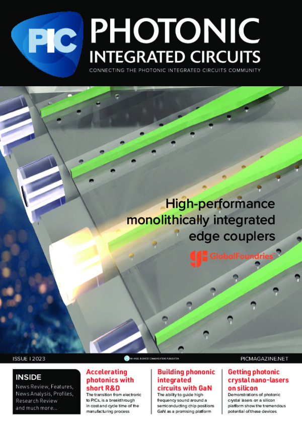
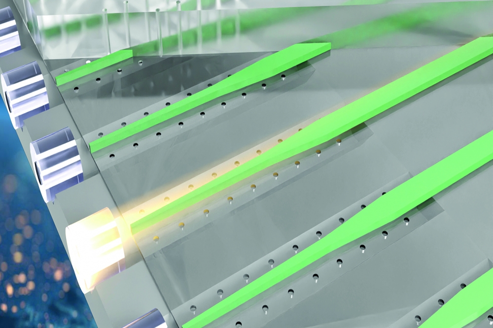
High-performance monolithically integrated edge couplers
Monolithic silicon photonics (SiPh) technology enables the large-scale fabrication of state-of-the art photonics and CMOS devices on the same silicon-on-insulator (SOI) substrate with ultra-low parasitics, allowing to build faster, and more energy efficient transceivers than the conventional hybrid integrated solutions. The realization of scalable, cost-effective and power-efficient optical inputs/outputs (I/Os) on the monolithic SiPh platform remains a significant challenge. In this article, GlobalFoundries researchers report on recent advances in their monolithically integrated high-performance edge coupling solutions, including V-groove-based fiber attach and cavity-based laser attach leveraging hybrid flip-chip bonding.
BY YUSHENG BIAN, TAKAKO HIROKAWA, KOUSHIK RAMACHANDRAN, KAREN NUMMY, KEN GIEWONT AND TED LETAVIC, GLOBALFOUNDRIES
The ever-increasing demand in global data communication is driving the emergence of low-cost, disruptive interconnect solutions that can simultaneously meet the energy consumption, bandwidth and throughput requirements. SiPh based optical interconnection technology has been widely recognized as a key enabler to overcome the power and bandwidth capacity bottlenecks encountered by its electrical counterparts [1].
The well-established complementary metal oxide semiconductor (CMOS) manufacturing infrastructure, along with many intrinsic advantages of Si material such as high refractive index and optical transparency, has rendered SiPh a viable solution towards high-performance, cost-effective, and mass-manufacturable photonic integrated circuits (PICs).
Moreover, the ability to implement wavelength division multiplexing and advanced modulation schemes, in conjunction with high performance electronic components and CMOS-compatible materials onto the SiPh platform has further enabled unprecedented bandwidth scalability and naturally led to complex photonic systems suitable for a variety of applications such as datacom, telecom, automotive LiDAR, artificial intelligence, quantum computing and bio-chemical sensing.
Monolithic SiPh platform
Among the existing SiPh solutions that have been demonstrated so far, monolithic SiPh technology has been identified as one of the most promising candidates to simultaneously meet the scalability, power consumption and cost efficiency demands for the next generation optical interconnection schemes [2]. By enabling the large-scale fabrication of state-of-the art photonics and CMOS devices on the same SOI substrate, monolithic SiPh technology holds great potential for ultra-low parasitic integration [3], and allows to build faster, and more energy efficient transceivers than the conventional hybrid integrated solutions leveraging 2.5D or 3D packaging [4].

Figure 1. Monolithic SiPh platform simultaneously integrating advanced photonic devices and CMOS components on the same SOI substrate.
Fig. 1 shows the cross-section of a representative monolithic CMOS SiPh platform. By leveraging dual Si thicknesses and dual contact modules, this platform enables seamless integration of the best-in-class active and passive photonic devices with high-speed CMOS transistors. The front end of line (FEOL), middle of line (MOL) and back end of line (BEOL) of the stack-up are co-optimized for both photonics and electronics, while satisfying stringent integration requirements and maintaining excellent fabrication fidelity for all the pre-existing devices with varying feature sizes. The RF-friendly BEOL stack is highly attractive for building complex logic circuits, high-Q inductors and low-loss transmission lines, while simultaneously serving as high-quality contact interfaces for advanced active photonic devices.
The incorporation of silicon nitride (SiN) material has further enriched the capability of the monolithic SiPh platform [5]. Benefiting from the optimized stack-up and integration flow, low-loss and robust SiN passive photonic components can be realized, with extended capabilities in nonlinear loss mitigation, high power handling and thermal stabilization. Moreover, the combination of Si and SiN waveguides (WGs) provides additional degrees of design freedom to enable a variety of advanced devices featuring expanded functionalities such as low loss waveguiding, efficient polarization management, compact interlayer transition, high performance edge and vertical coupling with optical fibers, to name a few [6].
Monolithically integrated fiber attach solution
A high-performance optical I/O interface that allows for the efficient coupling with a standard single mode fiber (SMF) or fiber array has been recognized as a key enabler to improve the scalability and cost efficiency of SiPh interconnects. To realize robust and highly efficient fiber to PIC coupling on the monolithic platform, advanced crystallographic etch module and state-of-the-art 300mm manufacturing processes are adopted to form high quality V-grooves with high structural yield that allow high accuracy fiber attach with passive alignment.
To enable efficient coupling between the SMF and edge coupler (EC) while preventing mode leakage into the substrate, the BEOL cladding above the spot size converter (SSC) is replaced with a thick, homogeneous dielectric layer, and the Si substrate underneath is partially removed and filled with index matching liquid during the measurement (See Fig.1 and Figs.2 (a)-(b)).

Figure 2. Monolithically integrated fiber attach solution. (a) 3D perspective view of SiN ECs. (b) SEM image of a V-groove arrayattached with SMFs. (c) Through-band insertion loss. (d) OFDR spectrum. (e) High power measurement results
At OFC2020, we reported the demonstration of low-loss fiber attach on our monolithic SiPh platform, which leverages Si metamaterial SSCs to significantly improve the fabrication and assembly tolerances over traditional designs using solid inverse tapers [7]. Statistical data of the insertion losses (ILs) and early reliability assessment results were presented for two types of edge couplers (i.e. low optical return loss (ORL) and low polarization-dependent loss (PDL) SSCs), which are optimized for the transmitter and receiver circuits, respectively.
As SiPh begins to penetrate various emerging areas such as LiDAR and quantum computing, the ability of an optical I/O to handle high optical power while maintaining other performance metrics becomes increasingly important to address the unprecedented demands in performance scaling and power consumption reduction.
These challenging requirements call for an alternative SiPh I/O solution other than the conventional EC schemes utilizing Si because Si as a material inevitably suffers from nonlinear effects that can potentially cause irreversible physical damage and excess loss at high optical power. Recently, by leveraging the SiN WG layer in the stack-up and incorporating additional process optimizations along with advanced free-form optical proximity correction, we realized for the first time, a low-loss, V-groove-based self-aligned SiN EC solution on our monolithic SiPh platform. This work will be presented at OFC 2023 [8].

Figure 3. III-V laser integration on the monolithic SiPh platform. (a)-(d) 3D perspective views of various PICs with different SSCs formed on Si or SiN layer. (e)-(f) Optical image and SEM of laser cavities with and without flip-chip-bonded laser. (g)-(j) Light- current curve, RIN, spectral characterization and SMSR performance. (k)-(l) Wafer-level accelerated reliability test results
Figs.2 (c)-(e) depict the measurement results of the SiN EC, which were extracted from a V-groove-based test structure comprising two ECs and a loop-back SiN WG. Fiber-attached chips using index matching fluid were prepared for both low-power and high-power measurements. With the assistance of a polarization controller to adjust the input polarization, the insertion loss and back reflection of the SiN EC can be measured separately by switching between the transmission and reflection modes of an optical vector analyzer (OVA).
The measured SMF to SSC IL spectrum shown in Fig.2 (c) clearly reveals a reasonable through-band performance over a 60 nm bandwidth centered at 1300 nm. <0.6 dB/0.8 dB IL for the TE and TM modes, along with a low PDL (<0.28 dB) and low wavelength dependence (<0.24 dB) were achieved simultaneously. Optical Fourier domain reflectometry (OFDR) centered at 1310 nm was then used to measure the back reflection of the loopback structure and the recorded spectra were converted into the spatial domain.
As illustrated in Fig.2 (d), two reflection peaks were observed near the input and output fiber facets. Based on the integrated reflection loss at the input facet, the back reflection at the first SMF-SSC interface was estimated to be less than -39 dB, which is a clear indication of the low ORL of the SiN EC.
Finally, the power handling capability of the EC was evaluated through ramping up the input laser power up to 520 mW. The measurement results shown in Fig. 2 (e) clearly reveals a linear relation between the input and output powers and the high-power tests were repeated to assure that there was no permanent physical damage or power-dependent loss in the PIC. These results further confirmed the robustness of the monolithically integrated SiN EC for high power applications.
Laser Attach Solution on the monolithic platform
As an indirect bandgap material, Si lacks the ability to emit light efficiently. The need to overcome such a challenge has led to the advent of various techniques with the aim of integrating other light-emitting materials onto the SiPh platform to enable low-cost and power-efficient on-chip lasers. By leveraging advanced flip-chip bonding techniques and butt-coupling scheme, we demonstrate the hybrid integration of III-V laser on our monolithic SiPh platform. The work was presented at OFC2021 [9] and more recently published on IEEE Journal of Selected Topics in Quantum Electronics as an invited paper [10].
A key feature to enable hybrid laser integration onto the monolithic platform is a precisely controlled laser cavity formed during the far BEOL processing (Fig.1). High-precision alignment of the laser can be realized by taking advantage of precise optical and mechanical features, allowing efficient direct butt-coupling of the laser beam into the SSC (Figs.3 (a)-(d)). This laser attach involves alignment and placement of the laser, followed by a laser-assisted solder reflow process to create p- and n-electrical connections to the laser.
The dimensions of the Si cavity are precisely controlled by using the locations of the SSC and the active multi-quantum-well region of the laser as references. A sub-micron accuracy pick-and-place soldering process enables precise alignment of the laser inside the cavity by utilizing high-precision alignment fiducials on the laser and SiPh chip. Standoff structures incorporating the existing layers are formed within the cavity, which serve as a mechanical stop feature allowing for the accurate vertical alignment of the laser. The metallization step is conducted to form the wiring levels within the cavity and provides lithographically defined solder connections that align and electrically connect with the p and n bottom contacts on the laser. The solder connections within the cavity also provide mechanical support and a thermal pathway for the laser during operation.
One key aspect of this scheme is the formation of a wiring level that steps up from the bottom of the cavity to the surface wiring levels of the PIC that are typically deployed for standard wire-bonding via last-metal bond pads or flip-chip interconnection through copper pillar receive pads. This unique approach enables standard electrical I/O to power the laser in a direct flip-chip configuration inside the cavity without the need for any additional assembly steps such as wire-bonding.
Figs. 3 (e) and 3 (f) show the optical image and SEM of a monolithic SiPh chip incorporating laser cavities and flip-chip-bonded lasers. Figs. 3 (g)-(j) depict the key performance metrics of the laser obtained from a series of wafer-level and module-level electro-optical testing. The coupling performance was evaluated by powering up the laser at 100 mA driving current and measuring the optical power output through both grating couplers and V-groove-based edge couplers.
The testing result shown in Fig. 3 (g) indicates > 14 mW optical power was coupled into the Si WG with the assistance of the inverse taper illustrated in Fig.3 (a). By switching to a stacked Si-SiN SSC design (Fig. 3(b)), over 20 mW output was measured at the WG. The pure-SiN-based alternative SSC options illustrated in Figs.3(c)-(d) are currently being evaluated for high power applications and the results will be reported in the near future.
Fig.3 (h) depicts the measured relative intensity noise (RIN) power spectral density as a function of the frequency for various externally added back-reflections (BRs). The stable laser performance at low levels of BRs and relaxation oscillations observed when power exceeds the laser BR tolerance clearly indicate that components in the optical path within the PIC did not negatively impact the RIN performance of the laser.
The spectral characterization result in Fig. 3 (i) shows the peak wavelength of the laser as a function of the bias current from a mode-hop-free module, indicating no evidence of any wavelength discontinuity. We also confirmed that no mode competition was occurring during the laser operation by monitoring the side-mode suppression ratio (SMSR), which remains above 50 dB in the operating range as illustrated in Fig. 3 (j).
Finally, we performed a series of reliability assessments on laser-attached Si submounts and SiPh cavity test vehicles to understand the long-term performance stability of the PIC [10]. The reliability results shown in Figs.3 (k)-(l) reveals stable performance throughout the stress testing, which further confirms the robustness of the laser integration on the monolithic SiPh platform.
Summary
In this article, we have provided a brief overview of the recent progress that was made in high performance edge coupling solutions on our monolithic SiPh platform, including V-groove-based self-aligned fiber attach leveraging Si and SiN SSCs, and hybrid integration of III-V lasers. The I/O techniques presented here can be readily scalable to an optical source array with high fiber or laser counts as well as fine pitches. Their full compatibility with automated high-throughput microelectronic packaging tools renders themselves as highly attractive candidates for complex photonic systems and co-packaged optical modules.
Reference
[1] R. Soref, “The past, present, and future of silicon photonics,” IEEE J. Sel. Topics Quantum Electron., vol. 12, no. 6, pp. 1678-1687, Nov. - Dec. 2006, doi: 10.1109/JSTQE.2006.883151.
[2] V. Stojanović et al., “Monolithic silicon-photonic platforms in state-of- the-art CMOS SOI processes,” Opt. Express, vol. 26, no. 10, pp. 13106–13121, 2018.
[3] K. Giewont et al., “300-mm monolithic silicon photonics foundry technology,” IEEE J. Sel. Topics Quantum Electron., vol. 25, no. 5, Sep. 2019, Art. no. 8200611.
[4] M. Rakowski et al., “45nm CMOS silicon photonics monolithic technology (45CLO) for next-generation, low power and high speed optical interconnects,” in Proc. Opt. Fiber Commun. Conf. Exhibi., San Diego, CA, USA, May 13, 2020.
[5] Y. Bian et al., “Towards low-loss monolithic silicon and nitride photonic building blocks in state-of-the-art 300mm CMOS foundry,” in Proc. Frontiers Opt., pp. paper FW5D. 2, Sep. 2020.
[6] Y. Bian et al., “Monolithically integrated silicon nitride platform,” Optical Fiber Communications (OFC), Th1A.46, San Diego, CA, USA, June, 2021.
[7] B. Peng et al., “A CMOS compatible monolithic fiber attach solution with reliable performance and self-alignment,” in Proc. Opt. Fiber Commun. Conf. Exhibi., San Diego, CA, USA, May 13, 2020.
[8] Y. Bian et al., “Monolithically integrated self-aligned SiN edge coupler with <0.6/0.8 dB TE/TM insertion loss, <-39 dB back reflection and >520 mW high-power handling capability,” Optical Fiber Communications (OFC), M3C.3, 2023.
[9] Y. Bian et al., “Hybrid III-V laser integration on a monolithic silicon photonic platform,” Optical Fiber Communications (OFC), M5A.2, San Diego, CA, USA, June, 2021
[10] Y. Bian et al., “3D Integrated Laser Attach Technology on a 300-mm Monolithic CMOS Silicon Photonics Platform,” IEEE J. Sel. Topics Quantum Electron., Invited Paper, vol. 29, no. 3, May/June. 2023, Art. no. 8200519. DOI: 10.1109/JSTQE.2023.3238290
Acknowledgement
The authors would like to thank Vaishnavi Karra, Abdelsalam Aboketaf, Thomas Houghton, Keith Donegan, Massmio Sorbara, Kevin Dezfulian, Francis Afzal, Zhuo-Jie Wu, Brian Popielarski,
Brittany Hedrick, Won Suk Lee, Ryan Sporer, Bo Peng, Shuren Hu, Steven Palmer, Janet Tinkler,
Robert Fox, Vikas Gupta, Anthony Yu and the rest of the GlobalFoundries team for their development engineering support for CMS90WG and 45SPCLO technologies.


