
Closing the 'terahertz gap'
EPFL researchers and colleagues from Harvard and ETH Zurich make thin-film terahertz photonic circuit
Researchers in EPFL'S Laboratory of Hybrid Photonics (HYLAB) have taken a step towards successfully exploiting the terahertz gap, which lies between about 300-30,000 GHz (0.3 to 30 THz) on the electromagnetic spectrum. This range is currently something of a technological dead zone, describing frequencies that are too fast for today’s electronics and telecommunications devices, but too slow for optics and imaging applications.
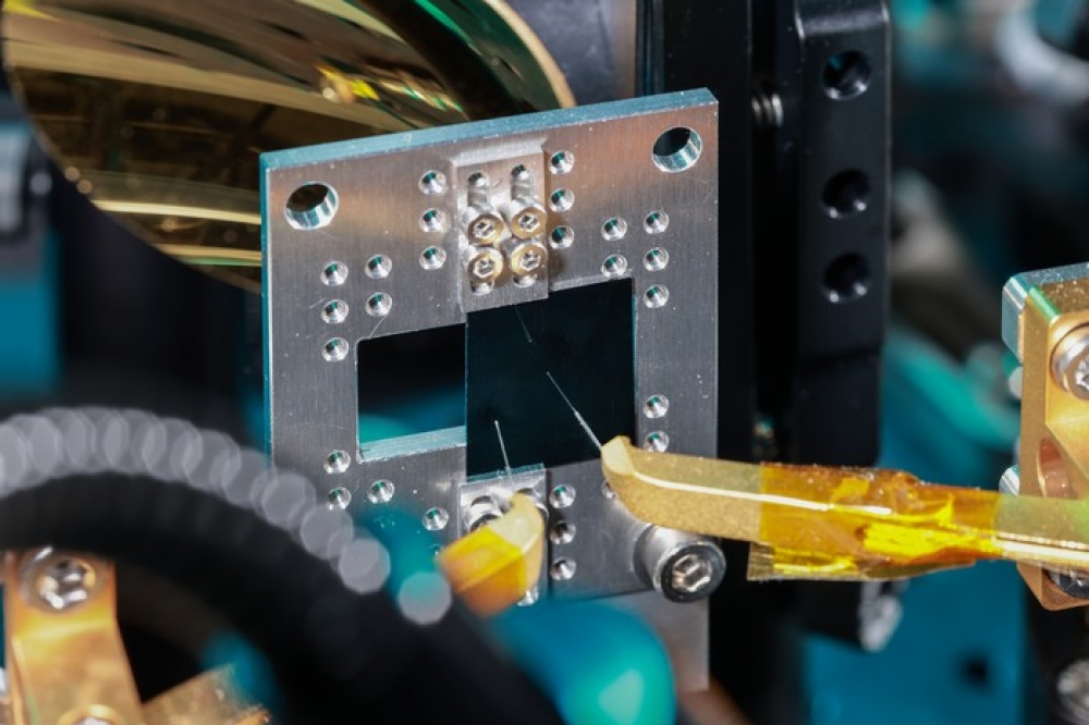
Led by Cristina Benea-Chelmus, the HYLAB researchers and colleagues at ETH Zurich and Harvard University have built an integrated photonic circuit made of lithium niobate that produces terahertz waves whose frequency, wavelength, amplitude, and phase can be precisely tuned.
Such precise control over terahertz radiation means that it can now potentially be harnessed for next-generation applications in both the electronic and optical realms. The results have recently been published in Nature Communications.
“Seeing the devices emit radiation with properties that we predefined was a confirmation that our model was correct,“ says co-first author Alexa Herter, currently a PhD student at ETH Zurich.
“This was made possible due to the unique features of lithium niobate integrated photonics,” adds co-first author Amirhassan Shams-Ansari, a postdoctoral fellow at Harvard University.
Telecoms-ready
Benea-Chelmus explains that while such terahertz waves have been produced in a lab setting before, previous approaches have relied primarily on bulk crystals to generate the right frequencies. Her lab’s use of the lithium niobate circuit, finely etched at the nanometer scale by collaborators at Harvard University, makes their novel approach much more streamlined. The use of a silicon substrate also makes the device suitable for integration into electronic and optical systems.
“Generating waves at very high frequencies is extremely challenging, and there are very few techniques that can generate them with unique patterns. We are now able to engineer the exact temporal shape of terahertz waves – to say essentially, ‘I want a waveform that looks like this,’” she explains.
To achieve this, Benea-Chelmus’ lab designed the chip’s arrangement of channels called waveguides, from which microscopic antennas broadcast terahertz waves generated by light from optical fibers.
“The fact that our device already makes use of a standard optical signal is really an advantage, because it means that these new chips can be used with traditional lasers, which work very well and are very well understood. It means our device is telecommunications-compatible,” Benea-Chelmus emphasizes. She adds that miniaturized devices that send and receive signals in the terahertz range could play a key role in sixth generation mobile systems (6G).
In the world of optics, Benea-Chelmus sees particular potential for miniaturised lithium niobate chips in spectroscopy and imaging. In addition to being non-ionizing, terahertz waves are much lower-energy than many other types of waves (like x-rays) currently used to provide information about the composition of a material – whether it’s a bone or an oil painting. A compact, non-destructive device like the lithium niobate chip could therefore provide a less invasive alternative to current spectrographic techniques.
“You could imagine sending terahertz radiation through a material you are interested in and analyzing it to measure the response of the material, depending on its molecular structure. All this from a device smaller than a match head.”
Quantum future
Next, Benea-Chelmus plans to focus on tweaking the properties of the chip’s waveguides and antennas to engineer waveforms with greater amplitudes, and more finely tuned frequencies and decay rates. She also sees potential for the terahertz technology developed in her lab to be useful for quantum applications.
“There are many fundamental questions to address; for example, we are interested in whether we can use such chips to generate new types of quantum radiation that can be manipulated on extremely short timescales. Such waves in quantum science can be used to control quantum objects.”
Reference
'Terahertz waveform synthesis in integrated thin-film lithium niobate platform' by Herter, A., Shams-Ansari, A., Settembrini, F.F. et al;. Nat Commun 14, 11 (2023)


