US centre to tackle processor energy efficiency

University of Illinois-based centre to focus on electrical and optical interconnects, heterogeneous 3D integration, and energy-efficient circuits
The US National Science Foundation is funding a centre for Aggressive Scaling by Advanced Processes for Electronics and Photonics (ASAP) housed at the University of Illinois's Holonyak Micro & Nanotechnology Lab (HMNTL).
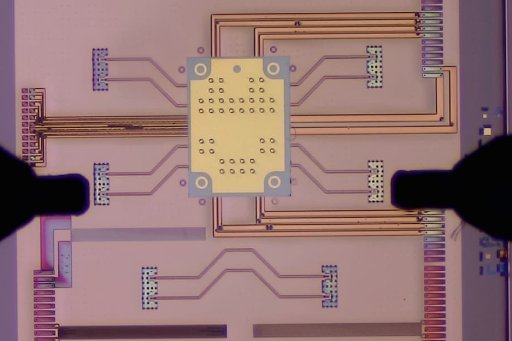
It will focus on electrical and optical interconnects, heterogeneous 3D integration, and highly energy-efficient circuits and architectures.
Director of the new centre, Shaloo Rakheja, an assistant professor in Electrical & Computer Engineering, HMNTL, says ASAP advances should improve the throughput of processing, resulting in faster speeds as well as lower energy use. “We want to basically improve on all fronts,” she says.
The biggest energy hog in microprocessors is the transmission of data: a complex fingernail-sized microprocessor might contain dozens of miles of copper interconnects through which data are moved. Typically, 50 percent to 60 percent of the energy consumption of microelectronics is due to interconnects, not due to actual computation; the percentage is even higher when data-intensive tasks, like image recognition, are being performed.
The ASAP will work as an Industry-University Cooperative Research Center (IUCRC) in which companies and other organisations pay annual dues to belong to the centre. The starting lineup of members includes national and DoD labs, large semiconductor foundries, chip manufacturers, software tool companies, and startups, among others.
Cliff Hou, SVP of R&D/Corporate Research at TSMC, said that “TSMC is dedicated to developing the cutting-edge process technology that the world will need in the future, and we are pleased to see that the centre for Aggressive Scaling by Advanced Processes for Electronics and Photonics is addressing research areas and associated concepts with great relevance for the semiconductor industry. We look forward to seeing the outcomes of the centre’s research with high hopes that they will help to propel the industry’s continuous quest for innovative technology scaling and greater power efficiency.”
“As microelectronics have evolved, IBM Research has retained its leadership in creating many of the industry’s newest technologies. Today, these advances are made in collaboration with a diverse ecosystem of public and private sector partners,” said Vijay Narayanan, IBM Fellow and Strategist, Physics of AI at IBM Research. “A full stack approach towards microelectronics research, such as this work with the centre for Aggressive Scaling by Advanced Processes for Electronics and Photonics, is critical to deliver system-level performance while maintaining energy efficiency, and we look forward to engaging closely with researchers in this centre.”


