High-performance Visible-light Lasers that Fit on a Fingertip

In a significant advance for impactful technologies such as quantum optics and laser displays for AR/VR, Columbia Engineering’s Lipson Nanophotonics Group has invented the first tunable and narrow linewidth chip-scale lasers for visible wavelengths shorter than red.
As technologies keep advancing at exponential rates and demand for new devices rises accordingly, miniaturizing systems into chips has become increasingly important. Microelectronics has changed the way we manipulate electricity, enabling sophisticated electronic products that are now an essential part of our daily lives. Similarly, integrated photonics has been revolutionizing the way we control light for applications such as data communications, imaging, sensing, and biomedical devices. By routing and shaping light using micro- and nanoscale components, integrated photonics shrinks full optical systems into the size of tiny chips.
Despite its success, integrated photonics has been missing a key component to achieve complete miniaturization: high-performance chip-scale lasers. While some progress has been made on near-infrared lasers, the visible-light lasers that currently feed photonic chips are still benchtop and expensive. Since visible light is essential for a wide range of applications including quantum optics, displays, and bioimaging, there is a need for tunable and narrow-linewidth chip-scale lasers emitting light of different colors.
Inventing high-performance lasers that fit on a fingertip
Researchers at Columbia Engineering’s Lipson Nanophotonics Group have created visible lasers of very pure colors from near-ultraviolet to near-infrared that fit on a fingertip. The colors of the lasers can be precisely tuned and extremely fast – up to 267 petahertz per second, which is critical for applications such as quantum optics. The team is the first to demonstrate chip-scale narrow-linewidth and tunable lasers for colors of light below red -- green, cyan, blue, and violet. These inexpensive lasers also have the smallest footprint and shortest wavelength (404 nm) of any tunable and narrow-linewidth integrated laser emitting visible light. The study, which was first presented at the CLEO 2021 post-deadline session on May 14, 2021, was published online December 23, 2022, by Nature Photonics.
“What’s exciting about this work is that we’ve used the power of integrated photonics to break the existing paradigm that high-performance visible lasers need to be benchtop and cost tens of thousands of dollars,” says the study’s lead author Mateus Corato Zanarella, a PhD student who works with Michal Lipson, Higgins Professor of Electrical Engineering and professor of applied physics. “Until now, it’s been impossible to shrink and mass-deploy technologies that require tunable and narrow-linewidth visible lasers. A notable example is quantum optics, which demands high-performance lasers of several colors in a single system. We expect that our findings will enable fully integrated visible light systems for existing and new technologies.”
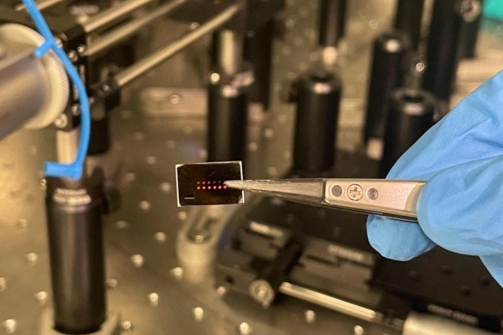
Illustration of the integrated laser platform created by the Lipson Nanophotonics Group, where a single chip generates narrow linewidth and tunable visible light covering all colors. Credit: Myles Marshall/Columbia Engineering
Benefits of emitting wavelengths below red
The importance of lasers emitting wavelengths shorter than red is clear when you consider some important applications. Displays, for example, require red, green, and blue light simultaneously to compose any color. In quantum optics, green, blue, and violet lasers are used for trapping and cooling atoms and ions. In underwater Lidar (Light Detection and Ranging), green or blue light is needed to avoid water absorption. However, at wavelengths shorter than red, the coupling and propagation losses of photonic integrated circuits increase significantly, which has prevented the realization of high-performance lasers at these colors.
Solving coupling and propagation loss issues
The researchers solved the coupling loss problem by choosing Fabry-Perot (FP) diodes as the light sources, which minimizes the impact of the losses on the performance of the chip-scale lasers. Unlike other strategies that use different types of sources, the team’s approach enables the realization of lasers at record-short wavelengths (404 nm) while also providing scalability to high optical powers, FP laser diodes are inexpensive and compact solid-state lasers widely used in research and industry. However, they emit light of several wavelengths simultaneously and are not easily tunable, preventing them to be directly used for applications requiring pure and precise lasers. By combining them with the specially designed photonic chip, the researchers are able to modify the laser emission to be single-frequency, narrow-linewidth, and widely tunable.
The team overcame the propagation loss issue by designing a platform that minimizes both the material absorption and surface scattering losses simultaneously for all the visible wavelengths. To guide the light, they used silicon nitride, a dielectric widely used in the semiconductor industry that is transparent for visible light of all colors. Even though there is minimal absorption, the light still experiences loss due to unavoidable roughness from the fabrication processes. The team solved this problem by designing a photonic circuit with a special type of ring resonator. The ring has a variable width along its circumference, allowing for single-mode operation characteristic of narrow waveguides, and low loss characteristic of wide waveguides. The resulting photonic circuit provides a wavelength-selective optical feedback to the FP diodes that forces the laser to emit at a single desired wavelength with very narrow linewidth.
“By combining these intricately designed pieces, we were able to build a robust and versatile platform that is scalable and works for all colors of light,” said Corato Zanarella.
Revolutionizing technologies
“As a laser manufacturer we recognize that integrated photonics will have a tremendous impact on our industry and will enable a new generation of applications that have so far been impossible,” said Chris Haimberger, director of Laser Technology, TOPTICA Photonics, Inc. “This work represents an important step forward in the pursuit of compact and tunable visible lasers that will power future developments in computing, medicine, and industry.”
The study’s findings could revolutionize a broad range of applications, including:
Quantum information
Atomic Clocks
Biosensing
Underwater Ranging
Li-Fi
Next steps
The researchers, who have filed a provisional patent for their technology, are now exploring how to optically and electrically package the lasers to turn them into standalone units and use them as sources in chip-scale visible light engines, quantum experiments, and optical clocks.
“In order to move forward, we have to be able to miniaturize and scale these systems, enabling them to eventually be incorporated in mass-deployed technologies,” said Lipson, a pioneer in silicon photonics whose research has strongly shaped the field from its inception decades ago, with foundational contributions in the active and passive devices that are part of any current photonic chip. She added, “Integrated photonics is an exciting field that is truly revolutionizing our world, from optical telecommunications to quantum information to biosensing.”
About the Study
Journal: Nature Nanophotonics
The study is titled “Widely tunable and narrow-linewidth chip-scale lasers from near-ultraviolet to near-infrared wavelengths.”
Authors are: Mateus Corato-Zanarella, Andres Gil-Molina, Xingchen Ji, Min Chul Shin, Aseema Mohanty, Michal Lipson (all from the Department of Electrical Engineering, Columbia Engineering; Ji now at John Hopcroft Center for Computer Science, Shanghai Jiao Tong University; Shin a research scientist at Reality Labs, Meta; Mohanty at Department of Electrical and Computer Engineering, Tufts University)
This work was supported as part of the Novel Chip-Based Nonlinear Photonic Sources from the Visible to Mid-Infrared funded by the Army Research Office (ARO) under award no. W911NF2110286. The photonic chips fabrication was done in part at the City University of New York Advanced Science Research Center NanoFabrication Facility, in part at the Columbia Nano Initiative (CNI) Shared Lab Facilities at Columbia University, and in part at the Cornell NanoScale Facility, a member of the National Nanotechnology Coordinated Infrastructure (NNCI), which is supported by the National Science Foundation (Grant NNCI-2025233). M.C.S. is supported by the Facebook Fellowship Award.
M.C.Z., A.G.M, X.J., M.C.S., A.M., and M.L. are named inventors on US provisional patent application 63/275,141 regarding the technology reported in this article.
Photo Credit: Myles Marshall/Columbia Engineering


