Silicon photonics is driven by data center applications

Silicon photonic platform maturity and rapidly developing ecosystem will
drive a $5.4B datacom market in 2027. And new applications in multiple
markets could emerge as well in the future.
BY ERIC MOUNIER, PH.D., IS DIRECTOR OF MARKET RESEARCH AT YOLE INTELLIGENCE, PART OF YOLE GROUP.
Data Centre networking is currently undergoing profound evolution. This evolution in architecture has, in turn, significant implications for the technologies at the transceiver and chip levels. Very-short-reach optical interconnects are coming for High Power Computing (HPC) and new disaggregated architectures where computing, memory, and storage components will be separated is a new trend. The global optical transceiver industry remains very competitive, and competitors are racing to develop different techniques to overcome physical limits to achieve higher data rates. Two platforms are clearly emerging: InP and Silicon Photonics, which will coexist during the coming years. Silicon photonics will be central in data center evolution in the short-term for 100 G (already well implemented in data centers) and then for 400 G and 800 G pluggables. It will also be an enabling technology for the disaggregation of data centers and a possible future CPO approach.
Although the Covid-19 pandemic and the Ukraine-Russia crisis have strongly impacted the semiconductor supply chain, the effect has been less in silicon photonics than in other semiconductor markets. Indeed, silicon photonics is a low-volume wafer and strategic technology, so allocated capacity does not affect the global fabs’ capacity, which is generally much larger. So, silicon photonics continues to gain traction in the data center industry.
In the Silicon photonics 2022 report, we estimated that the value of the silicon photonics market was more than 20% of the optical transceivers market for datacom in 2021, which is still growing. It will be more than 30% in 2027. Silicon photonics is more used in short reach and is increasingly used for 500 m DR, but it is also more and more used with coherent technology entering datacom applications. There is also an increasing demand for 400ZR. It is interesting to see how telecom technologies (e.g. : coherent technology) are diffusing throughout the datacom industry today. And besides datacom, other applications are promising in computing, interconnects in data centers, and sensing.
We forecast the silicon photonics market will be more than $1B (Si photonics units) in 2027, with 62 million devices. This will only require a modest number of wafers, estimated at about 70k 12’’ eq. SOI wafers. Data center applications will have the largest share with $467M.
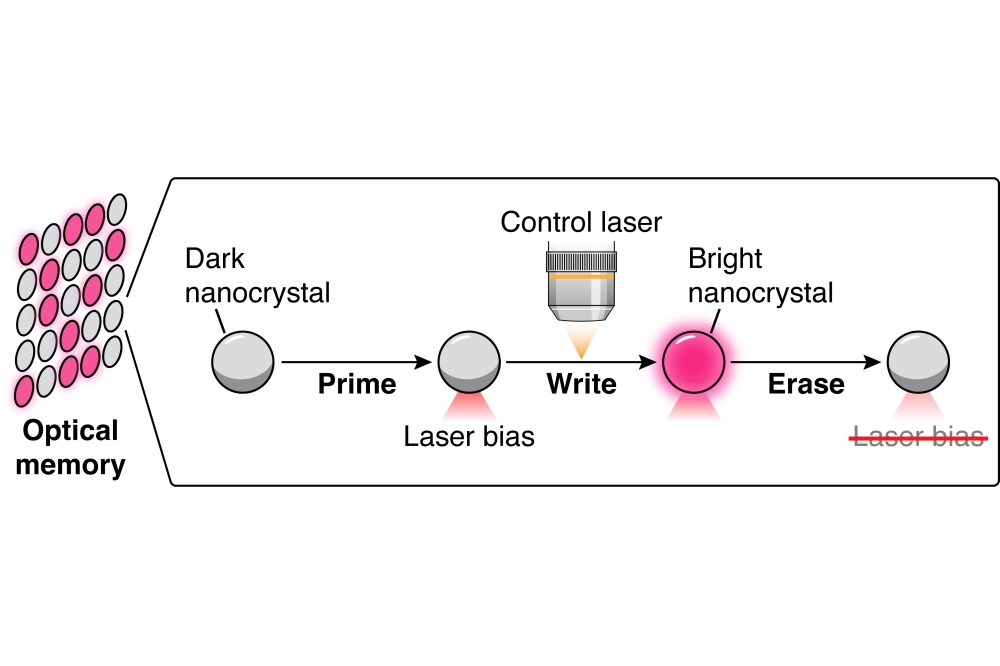
Optical interconnects will be $2M. Optical interconnects using silicon photonics will enable disaggregated data centers with more power available for high-performance computing (HPC) and data communications. This approach is pursued by AyarLabs, which is planning its first shipments in 2022. Applications will be HPC and data centers. Photonic computing, allowing for analog AI computations much faster than today’s digital AI is developing and will soon hit the market.
The market ramp-up for CPO is still an open question, but it will co-exist with pluggable optics. So far, Google and Meta (Facebook) have been defining their pluggable optics requirements based on switch performance. With both optical engines and switches in the same package and in the hands of the same player, GAFAMs would be highly dependent on suppliers such as Broadcom. CPO will likely be used initially for niche applications (such as custom-built high-performing computers) before massive adoption in datacom in the longer term.
Consumer health will be worth $240M. Consumer health development continues, with Rockley announcing shipments of its Pro module (VitalSpexTM) for 2022/23. This would pave the way for future integration of silicon photonics-based biosensors in wearables from large OEMs like Apple or Huawei. However, this is a complex technology to implement, and it is difficult today to say whether this approach will be widely used. Other applications include sensors (immunoassays, gyroscopes, and lidars ), 5G, optical processing, and CPO. Medical begins to hit the market, with Genalyte and many other startups using Si-integrated optics as a manufacturing platform. In the automotive domain, more and more manufacturers are integrating LiDAR into their products.
Player landscape
In recent years we saw strategic investments by both InP and Si photonics market leaders to strengthen their positions. The traditional InP-based players are strengthening their leading positions and are taking advantage of the platform for a new application – 3D sensing, and system vendors are betting on Silicon Photonics to enable scalable integration while eliminating the cost and complexity of the optical package.
In Si photonics, Intel is strengthening its market leadership with a 58% market share in units in 2021, followed by Cisco and other smaller companies (Marvell/Inphi, Sicoya, Acacia, and others) that, step by step, are gaining market share.
After decades of investments from Intel, the silicon photonics market is now the centerpiece of the evolution of the data center. Intel is now securing its access and manufacturing capabilities to leverage all its core competencies for the coming decades. From autonomous mobility to the data center and the future of cloud computing, Intel is now strengthening its position in the silicon photonics landscape with great recent results. From the decentralized on-the-edge central processing leader, Intel is transforming itself to be the centerpiece of the future of computing based on photonics and data centers.
The silicon photonics industrial landscape has remained very active. New potential applications of silicon photonics have resulted in the creation of various companies in the past three years. So, while some players are taking the opportunity to enter the optical transceiver market, others are looking for new applications: medical, sensors, interconnects, and computing. Co-packaged optics seem to require a large investment which is not achievable by any player yet, delaying its introduction. Maximum shipments of optical transceivers will probably occur only after 2026. This will push players that cannot get into co-packaged optics to move to new applications in 5 - 10 years. We should, therefore, see a shift in applications in the coming years.
China continues to be very active in the development of silicon photonics, with many players involved. It has invested heavily in silicon photonics manufacturing platforms and InP. The China-US trade restrictions and ZTE’s ban may prompt China to increase its support for high-speed optical chips, and domestic optical chip production is expected to accelerate further. Many companies worldwide are offering foundry services. The acquisition of Tower by Intel could lead to the creation of a major silicon photonics player.
Technology landscape
Historically, integrated photonics has been developed on an SOI platform. The goal was to leverage wafer-scale manufacturing from the CMOS industry and use it for photonic chips. But SOI is expensive, and silicon is not the perfect material for all the different photonics functionalities. Since the very start, the laser has been one of the greatest challenges for silicon photonics. The considerable development effort made by Intel for InP chiplet integration on SOI has been key to Intel’s actual business success in silicon photonics. More companies are now trying to duplicate this model to offer Si photonic wafers with integrated laser chips.
Today, as data rates increase, high-speed modulation using Mach-Zehnder on Si is becoming a bottleneck. There are numerous developments in new materials to overcome the current limitation (LNO thin films, InP, BTO, polymer, plasmons). For example, Arista has integrated thin film LNOs in modulators in an 800G transceiver prototype shown at OFC 2022.
This creates opportunities for companies focusing on materials for silicon photonics: Lumiphase and Polariton (created in Switzerland in 2019), Hyperlight and Liobate in China for thin film LNO, or Riber for BTO.
As integrated optics moves towards increased functionalities, the definition of Si photonics would broaden to incorporate other materials. Meanwhile, packaging and testing remain severe challenges for photonics. Current developments are being made to speed up testing time at the wafer level for Si photonic chips.
Conclusions
Silicon photonics as a platform is definitely a technology that will drive the datacom market in the coming years. It is also an enabling technology for co-packaged optics and possible new applications besides data centers. Silicon photonics is now a well-established technology and market, with more than 9 million silicon photonic transceivers shipped for data centers in 2021. In 2027,
It will be about 30% of the optical transceivers market in US$ value. Photonic processing could also be an important application of silicon photonics. Other applications include optical interconnects for disaggregated data centers. The industry is preparing for co-packaged optics (CPO), which is expected to arrive only after 2025.About the author
Eric Mounier, Ph.D., is Director of Market Research at Yole Intelligence, part of Yole Group. With more than 30 years’ experience within the semiconductor industry, Eric provides daily in-depth insights into current and future semiconductor trends, markets, and innovative technologies. Based on relevant methodological expertise and a strong technological background, Eric works closely with all the teams at Yole to highlight disruptive technologies and analyze and present business opportunities through technology & market reports and custom consulting projects. With numerous internal workshops on technologies, methodologies, best practices, and more, Eric ensures the training of Yole’s Technology & Market Analysts. In this position, he has spoken at numerous international conferences, presenting his vision of the semiconductor industry and the latest technical innovations. Previously, Eric held R&D and Marketing positions at CEA Leti (France). Eric Mounier has a PhD. in Semiconductor Engineering and a degree in Optoelectronics from the National Polytechnic Institute of Grenoble (France).”
About Yole Intelligence
Yole Intelligence is a consulting firm specializing in the strategic analysis of markets, the supply chain, and technological developments related to the semiconductor industry and adjacent industries. Benefiting from direct access to major players in the field of semiconductors and the multidisciplinary profile (scientific, technical, and market-oriented) of these analysts, Yole Intelligence supports its clients in the understanding of markets, the evolution of technologies, and their implementation in industry. The company provides its expertise through regular analyses and advice in strategic marketing and technical analysis. Yole Intelligence is part of Yole Group, with 180+ people worldwide. Yole Intelligence works closely with other group entities and partners. More information on www.yolegroup.com


