
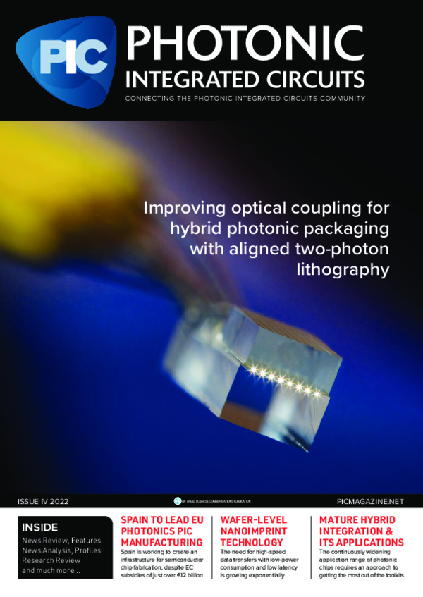
The best of both worlds: Mature hybrid integration & its applications

The continuously widening application range of photonic chips requires a practical approach to getting the most out of the available toolkit. Hybrid integration of photonic platforms is a versatile way of scaling module production with optimal performance.
By LIONiX INTERNATIONAL
With the commercial success of integrated photonics continuing apace, the industry continues to search for methods to streamline production while boosting its chips’ unique advantages. One persistent source of inspiration for integrated photonics is integrated circuits. In the history of integrated circuit development, the use of a single chip to integrate many electronic functions was definitional in its success.
This monolithic integration is a much sought-after goal within integrated photonics. At the same time, this makes monolithic integration of photonic integrated circuits (PICs) a legacy ambition. It should seem odd that the future of a novel technology is envisioned in its ability to replicate the success of a former one, but the reasons are sound enough that this strangeness is overlooked. Monolithic integration would lower production costs of PICs and centralize many of its processes. As of now, it remains an ambition.
With the various advantages that different photonic platforms over each other, it seems unlikely that one platform will rule them all. The functions built into photonic modules need both active and passive platforms, often requiring different platforms of the same kind to achieve the best performance. Fusing the platforms together after initial processing to create a single block of functional materials became the surrogate goal. Heterogenous integration has advantages of its own, most clearly in terms of the total size of the devices.
However, it also has its own unique challenges: how do we engineer dependable paths past different materials reacting to various conditions differently? New attempts at answering this question are published in peer reviewed journals daily. Once those arrive at a consensus, new machines and processes that can replicate these methods at high volumes must be invented to make heterogenous integration cost effective. This was also the case with electric circuits- only at massive quantities did the margins on monolithic chips make business sense.
In the meantime, a more direct and ultimately practical approach to the incorporation of different platforms exists in hybrid integration. The difference is subtle: in hybrid integration, the different photonic platforms remain separate, but are connected to each other. There are various advantages to this approach.
To start with, hybrid integration techniques have ceased to be experimental years ago. In most cases, they are simple reapplications of CMOS techniques, with alterations to fit the light-based operations of PICs. The performance these techniques deliver is reproducible. The yields of the processes are known. They are also cheap, and many of the machines used for their automated execution are adapted from their CMOS counterparts. Active alignment machines are a prime example that keeps getting better.
Nonetheless, there are some affordances specific to the integrated photonic industry to consider. The simplest method to attach an optical fiber to a photonic chip, or to attach two photonic chips together, is to use an adhesive and stick them together. Butt-coupling of this kind requires very accurate alignment, as the slightest discrepancy can cause the light to be absorbed or reflected away.
The choice of adhesive is also critical, as organic glues can absorb light in the blue region of visible light. Another factor to consider is the mode field diameter of the light in waveguides of different platforms. Without accounting for different diameters across platforms and fiber optics, there will always be signal losses at the periphery. Suffice to say that hybrid integration itself requires extensive engineering to ensure low optical losses. Such best practices are optimized over many iterations of hybrid assembly for different applications. Out of such cumulative experience, certain applications can be identified as commonplace archetypes of the potential in integrated photonics altogether. The following are such exemplary case studies from our work in LioniX International.

Figure 1: Mature hybrid integration means chips are designed with the
final assembly in mind. Pictured is the assembly of photonic chips
manufactured for project SPACEBEAM [1], fixed onto a printed circuit
board and plugged in for characterization. The inset shows an early
render of the TriPleX® SiN chip in the center with the smaller InP chips
in purple and gold. The render was produced as part of the design phase
of the module.
Mature integration processes cut on development time
Indium phosphide (InP) is one of the better-known waveguide platforms deployed in integrated photonics. Its key asset is its ability to generate light. This makes InP chips ideal as gain sections or amplifiers. However, the optical losses within InP make it less ideal for passive waveguides or delay lines. Silicon nitride (SiN) has very low optical losses, but is a passive material unable to generate or detect light. Our own TriPleX® technology is a SiN-based platform that further lowers the losses of standard SiN. TriPleX® makes for an excellent platform for optical modulators and filters, so combining it with InP became standard practice for our designers.
Using InP as a gain section and TriPleX® as a modulator, we fabricated a tunable laser with a miniscule form factor that produces 90 mW of power with a linewidth of less than 1 kHz and tunability over the entire c-band [2]. Using in-house design expertise and careful polishing of the interfaces, we were able to lower the optical loss across each interface to 1 dB, with only 3 dB loss from the bare InP chip.
The external cavity of the TriPleX® chip hosts a phase modulator, micro-ring resonators for wavelength modulation, and a power controller. Using SiN’s broad transparency and these chip building blocks allowed the optimization of the laser to other wavelength ranges, such as near infrared (780 to 850 nm) and the visible (420 to 680nm) spectrum. This specialization of functions across the two photonic platforms granted the best of both worlds without cutting back on the advantages of integrated photonics.
Stuffing an antenna into a lunchbox
The first ever fully optical beamforming network (OBFN) was made by us in 2018. As neat as these assemblies looked, they came out of years of optimization work. In earlier days, chips were simply connected with wires, and the assembly process was anything but simple. Not only did these take a lot of time and effort to put together, they were also fragile products which had to be treated very gently during characterization. These were not ready for in-situ deployment.
By 2018, however, the picture had changed dramatically. By this stage, vertical integration was part and parcel of our work. PICs were designed with final assembly in mind, and their electronics and packaging were co-designed at the same pre-production stages.
Modules for the transmission and reception of radio frequencies were designed and assembled, with the TriPleX chips fabricated in house. The modules included lasers, such that optical signal generation and processing was handled within the assembly. Those lasers followed the same principle as was described in the earlier section: InP gain sections butt-coupled to TriPleX.
However, the TriPleX chips in these modules did more than tune light into a target range. By integrating another InP chip, this one acting as a modulator, to the TriPleX chip, the TriPleX acted as a central hub for the translating of the radio frequency signal into an optical signal and vice versa.
For transmission, a photodetector array was included to convert the optical signal into RF, and switch delays were used to collate the signal. For reception, microring resonators were used to apply continuous delay to the received signal, and photodetectors were not implemented to allow remoting. Fiber arrays were used as the optical interfaces for the assemblies. What was remarkable even then was that the chips used in these assemblies were all mass-producible. With only the assembly as a bottleneck, scalable volume production was possible.
Since then, the OBFN went through many iterations, especially as it was redesigned for different applications. The OBFN was deployed in the distribution of 5G signals in a wide area without the use of antennae, in groundstation technology for satellite communication as well as satellite-side and on airplanes. Photodetectors became standard in our OBFNs to ensure that they were RF-in, RF-out. They became smaller, cheaper, and more robust.

Figure 2: The evolution of hybrid integration for a tunable laser
module. The top image shows an early benchtop assembly of the gain chip
(left) and tuning SiN chip (center). To move to higher volume
production, the assembly and packaging of the chips was standardized,
such that the chips can easily fit in a 12-pin butterfly package (bottom
left). Other designs, such as a dual gain module, were easy to
implement using similar processes (bottom right).
Scaling production for consumer markets
In the earlier examples, the low loss performance of the assembly is crucial to their function. The butt-coupling approach is favored in them for that reason, as active alignment can ensure the low losses necessary. Such markets can handle high end, medium volume applications.
To scale production to even higher volumes, new hybrid approaches are being developed. A common one is the etching of holes in the SiN wafers and then flip-chipping the semiconductor components into it [3]. This approach can be done at wafer scale through passive alignment. This enables its use for the high-volume quantities needed in telecommunications or consumer electronics applications. In the visible range, this process can be adapted for use in augmented reality (AR) glasses [4]. Red, green, and blue laser diodes can be flip-chipped onto the SiN wafer to make a light engine that combines the three laser modes into a single optimized one at the output. As no additional packaging is required, the light engine is very compact and manufacturable in high volumes.

Figure 3: The importance of a vertically integrated approach to photonic
module design. An early version of a photonic OBFN (top left) included a
SiN PIC but used common off-the-shelf components to connect it to
modulator s and electronics, resulting in a very bulky and fragile
device. Using a InP PIC modulator, hybrid integration allowed for the
construction of a much smaller device (top right). However, using wire
bonds to connect the chips and not codesigning its electronics meant
that the device was still fragile and bulky. By co-designing the PICs,
their assembly, and its electronics and interconnects, the device
achieved an assembly with thermal dissipation, mechanical stress relief,
and packageability (bottom). At the same time, the device is cheaper to
manufacture, easier to characterize, and is more powerful.
Therefore, hybrid integration includes many more techniques than simple butt-coupling. Micromachined mirrors can be placed at 45° angles to waveguides, allowing for vertical out-coupling of the light. Grating couplers allow the same thing, with the possibility of splitting the light by wavelength. Free space out-coupling allows for light interference effect to be engineered into applications. Nonetheless, what is crucial about hybrid integration is that it is functional. For the PIC industry to have a felt impact in technological advancement, techniques must exit the laboratory and be implemented in consumer-grade products. With multiple waveguide platforms being necessary, and monolithic fabrication in early research stages, hybrid integration unites different material properties with market-ready processes. It is the best of both present worlds.
References
[1] Manuel Reza, Giovanni Serafino, Tobias Otto, Ahmad Mohammad, Hakimeh Mohammadhosseini, Leili Shiramin, Francesco Floris, Matthias Kolb, Dave Bail, Simone Gabrielli, Chris Roeloffzen, Paul van Dijk, Amin Abbasi, Bart Desoete, and Paolo Ghelfi, “Design and Performance Estimation of a Photonic Integrated Beamforming Receiver for Scan-on-Receive Synthetic Aperture Radar,” J. Lightwave Technol. 39, 7588-7599 (2021)
[2] Lin, Y., Browning, C., Timens, R. B., Geuzebroek, D., Roeloffzen, C. G. H., Hoekman, M., Geskus, D., Oldenbeuving, R. M., Heideman, R. G., Fan, Y., Boller, K., & Barry, L. P. (2018). “Characterization of Hybrid InP- TriPleX Photonic Integrated Tunable Lasers Based on Silicon Nitride (Si 3N4/SiO2) Microring Resonators for Optical Coherent System,” in IEEE Photonics Journal, vol. 10, no. 3, pp. 1-8, June 2018, Art no. 1400108, doi: 10.1109/JPHOT.2018.2842026.
[3] Michael Theurer, Martin Moehrle, Ariane Sigmund, Karl-Otto Velthaus, Ruud M. Oldenbeuving, Lennart Wevers, Ferry M. Postma, Richard Mateman, Frederik Schreuder, Dimitri Geskus, Kerstin Wörhoff, Ronald Dekker, Rene G. Heideman, and Martin Schell, “Flip-Chip Integration of InP to SiN Photonic Integrated Circuits,” J. Lightwave Technol. 38, 2630-2636 (2020)
[4] Brilliance. Retrieved October 14, 2022, from https://www.brilliancergb.com


