
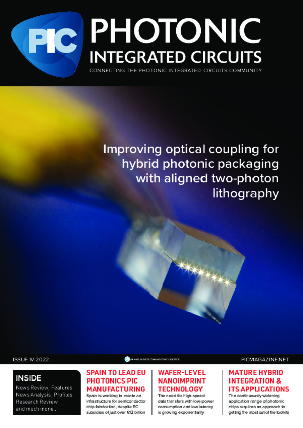
Improving optical coupling for hybrid photonic packaging
Nanoscribe’s 3D Microfabrication is a key enabling technology for the
optical coupling and packaging of photonic components in hybrid
integration to enable the penetration of photonic integrated circuits
(PIC) in industrial high-volume manufacturing.
BY JÖRG SMOLENSKI AND SOFÍA RODRÍGUEZ, NANOSCRIBE
Photonic data processing and photonic quantum computing have a great potential to exploit the concept of computing at the speed of light. For example, artificial intelligence (AI) applications demand high computing power and storage capacity. But electronic technologies currently struggle with the processing power needed in AI. New methods are under investigation by moving away from electronic towards photonic approaches for ultrafast information processing. Moreover, photonic integrated circuits extend also to application fields such as frequency-modulated continuous wave (FMCW) LiDAR, wearables, or medical and environmental sensors or data and telecom applications.
The challenge of hybrid integration in photonic packaging
Photonic packaging means integrating photonic integrated circuits (PIC) with a wide range of active and passive optical components into a compact module but with the key challenge to couple the light between each of them. The buildup is not monolithic as in electronics packaging but rather heterogenous with active alignment of the different components to each other. Next to the PIC itself, these components include lasers, photodiodes, waveguides, optical sensors, fibers and other optical modules. To integrate the different components, photonic packaging requires specialized microoptical structures as highly efficient optical coupling elements. These elements can couple light between various optical components and platforms, facilitating hybrid integration.

Figure 1: This image shows a lensed fiber array (LFA). Nanoscribe’s
Two-Photon Polymerization is used to print Free Space Microoptical
Coupling (FSMOC) elements directly on fiber arrays. Image: © PHIX Photon
Nanoscribe’s additive manufacturing technology of Two-Photon Polymerization (2PP) offers a unique microfabrication approach to tackle the issue of hybrid integration. The core capability of this technology is to 3D print finest miniature structures of virtually any shape. Its versatile capability to fabricate high-precision 3D structures on the nano- and microscale is an asset for developing microoptical coupling elements with specific designs. In 2PP technology, a pulsed laser is used to cure a photopolymer resin to create shapes with submicron resolution [1]. The technology enables the fabrication of free space microoptical couplers (FSMOC) with complex 3D geometries. Using 2PP’s 3D design freedom, FSMOC designs can be adapted to fit in with a variety of photonic packaging systems. The 3D printing capability of 2PP enables challenging microfabrication tasks for highly efficient light coupling onto different photonic platforms.
Relaxed alignment tolerances by 3D microfabrication
The different photonic components usually have different optical coupling interfaces (e.g beam diameter, numerical aperture, etc.) and also require different coupling strategies: the coupling between single components either occurs through the edge of the die (edge coupling) or through the surface (surface coupling). The most common technique for edge coupling is either with a lensed fiber or butt coupling. In the second, a fiber is directly positioned on the facet of the edge coupler. Lensed fibers enable simple mode field adaptation but are not usable for high volume production due to the optical lens design limitations (e.g. for elliptical mode fields).
Not only the variety of optical coupling interfaces require specifically designed microoptical couplers, also, another challenge of photonic integrated circuits in photonic packaging is to precisely align passively these optical components instead of the costly active alignment that has been the traditional approach. The challenge is relaxing alignment tolerances for packaging to several micrometers instead of hundreds of nanometers. Efficient optical coupling with active alignment is a time-consuming process. The 2PP technology is therefore a decisive microfabrication strategy that enables passive packaging (pick & place) by the use of non-contact FSMOC, allowing tolerances of a few micrometers for the final components. The difficulty of precise alignment in photonic packaging is transferred from the packaging process to the printing technology. 2PP has demonstrated to tackle these difficulties by printing microoptical coupling elements in place with an automatic alignment system with nanometer precision. The microoptical elements are directly printed on the optical interface of chips or fibers with a precision of down to 200 nm. The low alignment tolerances between optical elements mentioned above are achieved by simply tailoring the beam shapes and by making mode field adjustments. The design of FSMOC can be easily and quickly adapted to new requirements and applications. This flexibility takes into consideration the different types of microoptical fiber-to-chip couplers needed, for example for lensed fiber-to-chip, lensed chip-to-fiber and lensed fiber-to-lensed chip.
Aligned printing of microoptical couplers on fibers
Freeform microoptics can be 3D printed on fiber tips for imaging and beam shaping tasks, including challenging applications such as periscopic lenses used for wafer-level testing. There are different options to couple a fiber to other optical components, depending on the application. Using free space microoptical coupling (FSMOC) is a viable route to implement freeform optics for shaping light beams and coupling light from one to another optical component. Many applications require to steer and form beams from small to large or from large to small mode field diameters. The beams need to follow a path in different directions from a planar, to an inclined or even vertical direction.
FSMOC on fibers are used to tailor beams with beam expanders. For this purpose, freeform microlenses are 3D printed onto fibers using 2PP. One application example for printing onto fibers using 2PP is the case of a beam expander for a 25 µm mode field diameter. A fiber array with 460 HP single mode optical fibers is the starting optical platform. The camera-based detection is used to precisely detect the fiber core position before the printing within a ring down to 500 nm around the core. Then, the beam expanders are printed with automatic alignment to produce a lensed fiber array (LFA). To prove the performance of the microoptical couplers, the beam propagation is measured for 532 nm wavelength with a metrology setup. The measured beam coincides with the simulated expanded beam. The beam allows single mode fiber array to fiber array coupling over 1.2 mm. A 25 µm beam expander for 532 nm wavelength achieves ± 2.5 µm for 1 dB lateral alignment tolerance. This result demonstrates the precise performance of the camera-based alignment process for printing freeform microoptics to the core of the fibers, opening the way as a viable tool for research and industrial applications.
Moreover, the use of focusing lenses on fibers can generate a small beam output from a SMF fiber (e.g. fiber mode field diameter of 10 µm at 1550 nm). In this case the printed microlenses onto the fiber are focusing lenses that can achieve direct coupling to tapered waveguides with low coupling losses. A lens focusing to a mode field diameter of 3.6 µm achieves a loss of -1.7 dB per coupling interface on SMF28 fibers for 1550 nm for coupling to SOI tapered edge coupled waveguides.

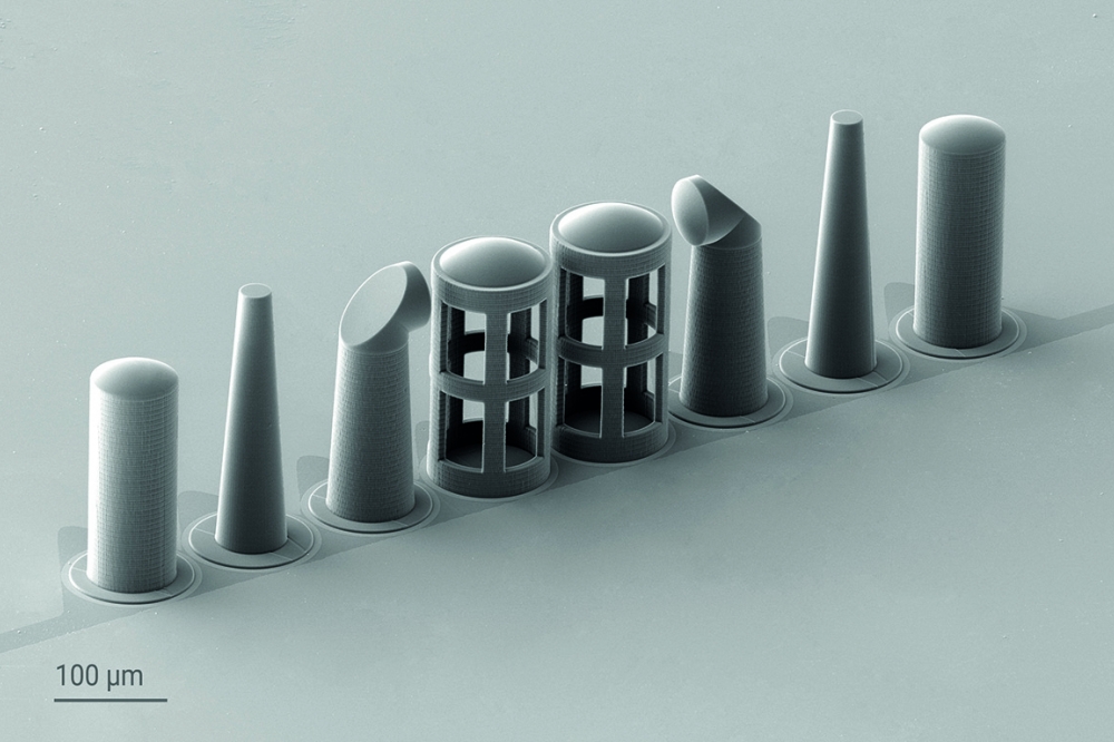
Figure 2: SEM image of different optical designs printed precisely
aligned to the fiber core in a v-groove fiber array. Image: © Nanoscribe
Aligned printing of microoptical couplers on chips
To fabricate optical couplers for edge coupling from a photonic chip to another die or towards a fiber, the spatial orientation of the fiber cores and photonic chips have to be detected. For this, 2PP-based 3D printers implement another automated method for aligned printing on chips: integrated confocal 3D mapping. The inline confocal imaging module provides a 3D mapping of the substrate topography. This enables precise lateral alignment, down to 200 nm, and precise 3D alignment to predefined markers or waveguides. Optical interfaces on photonic chips or fiber cores and their spatial orientation are automatically detected, and predefined freeform microoptics are printed directly in place. Thus, 2PP-based microfabrication reduces the complexity of the process chain, and assembly tolerances are relaxed while enabling even more compact devices. The often costly active alignment process is no longer necessary. Moreover, there is a strong need to reduce coupling losses between fibers, edge couplers, grating couplers, emitting facets, and especially between different material platforms. 2PP-printed microoptical couplers achieve lateral excess coupling losses down to 1 dB or below.

Figure 3: Free Space Microoptical Couplers are used for collimating
light beams with relaxed alignment tolerances, achieving coupling losses
of below 1 dB. Optical micrograph of the FSMOC on fiber array (left)
and simulated beam expansion (right). Source: Sample from research
project MiLiQuant © Nanoscribe
Quantum X align, Nanoscribe’s 2PP-based printer for photonic packaging is combining all the above mentioned features such as alignment with nanoprecision and novel printing processes for precisely aligned 3D printing on optical fibers and photonic chips. The system uses automatic detection of the printing base to measure the spatial orientation of the fiber cores or photonic chips. Using this detection system, the printer manufactures freeform microoptical components directly in place, facilitating optimized optical coupling on photonic platforms.

Figure 4: The SEM shows an example of beam shaping optics printed on a
photonic chip. Source: Sample from research project HandheldOCT ©
Nanoscribe
Additively manufactured freeform microoptics
Additive manufacturing by Two-Photon Polymerization allows to go beyond classical optical designs on the microscale. Nearly any three-dimensional shape, be it spherical, aspherical, sharply edgy, freeform, and even compound 3D microoptics composed by a stack of various lenses can be materialized with 2PP-based 3D printing. This capability circumvents limitations imposed by mechanical tools and geometrical and process design constraints known from subtractive techniques.
When printing 3D microstructures, the 3D objects are printed line by line to form one layer, and layer by layer to build the 3D shape. To achieve this discretization, the structure design is sliced in layers with a defined slicing distance using the print preparation software. Each microstructure can combine different elements, for example, one supporting base and a functional lens can be printed combined in one design and one pass. To reduce print time and reach best optical quality, each element is printed using different printing parameters. Thus, the supporting base will be printed with a coarse slicing setting while the lens structure will be printed with a much finer slicing.
This advanced printing strategy, called smart slicing, allows to reduce print time and achieve optically smooth surfaces. The resulting 2PP-printed microoptics have surfaces roughness Ra that reach down to less than 10 nm. Moreover the designs printed with this technology achieve a shape accuracy in the range of 200 nm or less.

Figure 5: In Two-Photon Polymerization, a sharp polymerization threshold
separates the polymerized from the unpolymerized areas within the
photoresin. Outside the focal volume, the intensity falls below the
polymerization threshold and thus the photoresin remains liquid. The
size of the polymerized voxel can be tuned with varying laser intensity,
which is the core capability of Two-Photon Grayscale Lithography (2GL
®) [2]. © Nanoscribe
Novel 3D microfabrication opportunities
2PP has been used for years mostly at universities and research organizations. Nanoscribe’s new industrial 3D printers make novel and advanced microfabrication capabilities such as 3D-aligned printing particularly attractive to the photonic packaging industry. With its versatility, the 2PP-based printers can overcome light transmission challenges in photonic packaging by adapting the mode field diameter from one material platform to another while optimizing coupling efficiency by reducing coupling losses.
The 2PP technology allows for fast photonic packaging by relaxed alignment tolerances between the optical components. In this respect, 3D-aligned additive manufacturing of microoptical elements is crucial for the penetration of photonic integrated circuits in high-volume industrial manufacturing. The explained advances will also have effects in diverse applications such as photonic computing and data processing for AI, sensing and imaging applications needed in automotive and medical fields.
References
[1] Additive manufacturing based on Two-Photon Polymerization. A key enabling technology for high-precision 3D printing. https://www.nanoscribe.com/en/whitepaper/
[2] Introducing Two-Photon Grayscale Lithography. Outstanding performance of a new maskless lithography technology. https://www.nanoscribe.com/en/whitepaper/


