Enabling next generation photonic integration and packaging solutions

With the growth of photonic integrated circuits comes the need to innovate quickly. This innovation acceleration is made possible by the creation of Photonic Wire Bonding. Much as electrical integrated circuits have benefitted from electronic wire bonding, photonics innovations will now advance on a faster trajectory. By Vanguard Automation GmbH, Karlsruhe, Germany
By Vanguard Automation GmbH, Karlsruhe, Germany
Enabling next Generation Photonic Integration and Packaging Solutions with Photonic Wire Bonding (PWB) and Facet-Attached Micro-Lenses (FAML).
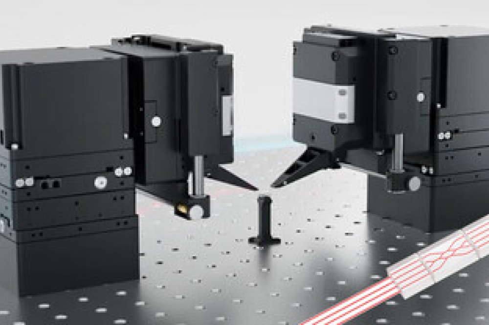
With the growth of photonic integrated circuits comes the need to innovate quickly. This innovation acceleration is made possible by the creation of Photonic Wire Bonding. Much as electrical integrated circuits have benefitted from electronic wire bonding, photonics innovations will now advance on a faster trajectory. Photonic Wire Bonding creates low-loss, 3D free-form connections between optical components. Built on advanced nano-print technology, Photonic Wire Bonding is inherently automatable and provides a high degree of design flexibility. Additionally, 3D nano-printing can also be used to fabricate facet-attached micro-optical elements on optical chips and fibers, allowing for low-loss coupling with high alignment tolerances and for wafer-level probing of optical devices.
Figure 1: Vanguard Automation’s fully automated photonic integration and
packaging solution vanguard SYMPHONY comprising the automated 3D
lithography based nano fabrication unit SONATA 1000 and the automated
pre- and postprocessing unit REPRISE 1000. The systems are equipped with
Vanguard’s BrightWire3D software enabling highly precise detection and
on the fly trajectory calculation. Vanguard’s own photoresists, standard
process development as well as product support and services complete
Vanguard’s solution for prototyping and mass production.
Today’s packaging and assembly challenges arise from the necessity to integrate various optical components from different material platforms. A hybrid module comprising, e.g., indium phosphite based active devices such as lasers or semiconductor optical amplifiers, passive devices made from silicon, silicon nitride or lithium niobate as well as photo diodes, and single mode or polarization maintaining fibers imposes a challenge in terms of integration due to their very specific optical properties.
A packaging or integration solution which is viable in industrial mass production has to be able to address and solve challenges arising from these specific optical properties. In order to reduce coupling loss when combining different devices, the specific mode field profiles have to be matched and the devices have to be aligned very precisely. For an industrial mass production process such mode matching and alignment processes have to be very fast and reproducible since speed and yield determine the cost of the product.
Additionally, the packaged assemblies must be reliable under various environmental conditions specific to their applications. These fundamental conditions hold true for a large range of application areas such as tele and data communication, 3D sensing, e.g, lidar as well as quantum applications while the application specific conditions which the packaged assemblies have to meet may vary. Thus, even though devices which are used for such applications are made in sophisticated processes from sometimes exotic material platforms, the optical packaging or integration process represents the biggest cost driver in most cases.
In order to solve this commercial challenge for next generation hybrid multi-chip modules the aforementioned technical challenges have to be resolved. Vanguard Automation has set out to advance photonic packaging and assembly by providing scalable 3D nano-fabrication solutions for prototyping and industrial mass production. Vanguard Automation GmbH is headquartered in Karlsruhe, Germany which is also home to the Karlsruhe Institute of Technology (KIT) and a fast-growing start-up scene. Vanguard started operating in 2018 as a joint venture combing a decade worth of research in silicon photonics and integrated optics from the group of Professor Christian Koos at KIT with 20 years of experience in building industrial machinery for assembly of opto-electronic components and (hybrid) photonic devices contributed by ficonTEC Service GmbH in Achim, Germany. Inspired by electronic wire bonding with its benefits such as fast process times, tight packaging density and loop control Christian Koos and his team of talented engineers developed a method of 3D nano-printed polymer waveguides so-called Photonic Wire Bonds (PWB).
Vanguard Automation then developed the photonic wire bonding technology further into a fully automated solution portfolio comprising two systems for fabrication of PWBs and postprocessing of connected optical assemblies, software for automated detection as well as calculation of optimal PWB trajectories, dedicated photoresists, standard processes as well as service and support (see Fig. 1) to enable customers to advance quickly.
In Vanguard’s systems single multi-chip assemblies, a tray with many assemblies, or wafers up to 12 inch can be handled which makes them viable for high-throughput production. In Vanguard’s SONATA 1000 systems the interfaces which have to be connected by PWBs are immersed in a special photoresist. Vanguard developed and tailored photoresists for specific requirements such as high resolution, strong adhesion on edge-facets and surfaces, and durability. In the SONATA 1000 the immersed devices are brought into contact with a high NA objective lens. This lens focuses a pulsed femtosecond laser into the resist.
First the laser is used to identify the interfaces as well as their orientations with an accuracy of sub 100 nm. Afterwards Vanguard’s Bridgewire3D software calculates the PWB trajectory on the fly based on the detected positions and orientations of the interfaces. Then the laser polymerises the photoresist along this trajectory by two photon polymerisation forming the optical connection between the interfaces. Hence, no calibration between detection and printing mechanism is necessary. Such a process comprising detection, calculation, and printing of a PWB is fully automated, reproducible and fast, which makes it viable for industrial mass production. The REPRISE 1000 system removes the unexposed resin, cleans the assembly and encapsulates the PWBs. The packaged assembly can then undergo follow-on processing (e.g. electric wire bonding).
The encapsulation process, or cladding, is done by detecting the PWB area, dispensing a dam, filling in the cladding material, and completed by UV-curing, either locally or with its 12 inch UV flood exposure. Therewith, Vanguard’s SYMPHONY comprising SONATA 1000 and REPRISE 1000 enables fully automated photonic packaging and integration of multi-chip assemblies or full wafers for industrial mass production using Photonic Wire Bonding or Facet-Attached Micro-Lenses or a combination of both. All processes on Vanguard’s systems are software defined and can be adapted to customer specific requirements. Vanguard Automation, offers process development either directly or through eco system partners who offer development of Photonic Wire Bonding processes adapted to customer assemblies with their own Vanguard systems. In addition, customers can benefit from Vanguard’s support and service contracts which, amongst other topics, provide access to PWB experts who assist with the adaption of fabrication processes to new devices.
Figure 2: left Scanning electron beam microscope image of Photonic Wire
Bonds connecting a single mode fiber array with an array of indium
phosphite based lasers from Vanguard’s partner FREEDOM PHOTONICS LLC (a
Luminar company). It has to be noted that the sample is tilted in order
to show the vertical offset between the components. right Scanning
electron beam microscope image of a Facet-Attached Micro-Lens on an
indium phosphite based laser.
Vanguard’s PWB technology is capable of addressing the fundamental challenges of photonic integration of multi-chip assemblies (see Fig. 2 left). Highly precise alignment of components is no longer necessary due to the highly accurate detection methods and algorithms in Vanguard’s systems. Additionally, vertical and/or lateral misalignments of up to +/- 20 µm of the optical interfaces are compensated by the s-shaped trajectories of PWBs (see Fig. 2 left). This allows for a fast pick and place process of components with relaxed placement tolerances rather than a more difficult and time consuming active-alignement process.
This also means that during the PWB writing process no active operation of devices is necessary. Mode-matching happens intrinsically in the process by free-form tapering of PWBs to adapt them to the device specific mode field profiles which can be round, elliptical or rectangular. As shown in Fig. 2 left, the PWB taper facing the single mode fiber (SMF) differs from the taper facing the indium phosphite based laser. Additionally, in case of angled facets or waveguides or rotated devices the PWB taper direction can be adjusted. In Fig. 2 left the PWB meets the laser facet under a specific angle determined by the different effective refractive indices of PWB and laser. Based on these properties PWBs connect various interfaces in multi-chip assemblies enabling a high degree of design flexibility for hybrid multi-chip integration. The software defined processes allow for a quick adaptation when devices have to be changed, e.g., for second sourcing or when devices are added to the product. Additionally, PWBs facilitate a high interconnect or package density due to their very compact size, which also lends itself to short fabrication times.
Vanguard’s Facet-Attached Micro-Lenses (see Fig. 2 right) round off Vanguard’s photonic integration and packaging solutions. They are a complementary approach to the Photonic Wire Bonds enabling free space optics over larger distances including low-loss coupling with high alignment tolerance. These lenses can be designed with a flexibility in shape including various lens surfaces and total internal reflective mirrors. They are precisely aligned and printed to the interface position and orientation using Vanguard’s highly accurate detection mechanisms. For wafer-level probing of optical devices Vanguard’s printed wafer-level probers are widely used in research and industry for several years. Hence, Vanguard’s wafer-level probers are used by market-leaders in their modern wafer-level probing systems proving the maturity of Vanguard’s technology portfolio for industrial applications.
Vanguard’s Photonic Wire Bonds as well as Facet-Attached Micro-Lenses have been successfully tested in a wide variation of environmental conditions such as standard Telcordia damp-heat and temperature shock/cycling tests (see Fig. 3), vibration tests, mechanical shock tests as well as for high-power handling, reflow soldering and die bonding. With respect to quantum applications, they also have been tested in low and ultra-low temperature environments.
Figure 3: left Telcordia damp heat test (85°C, 85% relative humidity)
result over 3500 hours of Photonic Wire Bonds. Each square represents
the average of several tens of PWB. right Telcordia thermal
shock/cycling test (temperature cycles of -40 – 85°C) result over 300
cycles of Photonic Wire Bonds. Each block represents the average of
several tens of PWB.
In summary, Vanguard’s Photonic Wire Bonding technology allows to combine the complementary strengths of different optical integration platforms in advanced photonic multi-chip modules leading to compactness, high performance, and great design flexibility. Vanguard’s portfolio is completed by Facet-Attached Micro-Lenses on optical chips and fibers, allowing for low-loss coupling with high alignment tolerance and for wafer-level probing of optical devices. All fabrication processes are fully-automated, highly reproducible as well as reliable and used by research and industry customers for next generation photonic integration and packaging.


