Spain could prioritize PIC manufacturing to lead in EU photonics

Spain is working to create an infrastructure for semiconductor chip
fabrication, but despite subsidies of just over €12 billion, Spain has
found it challenging to attract manufacturers. The European Photonics
Industry Consortium (EPIC) looks at the challenges involved and
opportunities for alternative investment in Spain’s vibrant Photonic
Integrated Circuits (PICs) ecosystem.
BY DR. IVAN NIKITSKIY, PHOTONICS TECHNOLOGY MANAGER, EUROPEAN PHOTONICS INDUSTRY CONSORTIUM (EPIC)
The race for semiconductors
Semiconductor chips are essential for all electronic devices and subsystems ranging from TVs, computers, and laptops to smartphones, vehicles, and medical diagnostic equipment; demand is so great that microchips are seen as the “new oil” of the 21st century.
However, over the last two decades, the global electronics industry has become increasingly dependent on semiconductor manufacturers in Taiwan, South Korea, and China, who, in 2019, accounted for 78% of the world’s semiconductor fabrication capacity. In light of the global semiconductor shortage that began in 2020, this dependency is now seen as a national security issue across both Europe and in the US. Accordingly, in February 2022, the US Congress approved the Chips and Science Act that allocated $52 billion to help US companies manufacture semiconductor chips with the aim of “re-establishing American leadership in the technology.” The EU followed suit in February 2022 with their own Chips Act comprising a pledge of €43 billion to reduce “excessive dependencies on Taiwan, the United States, South Korea, Japan and China” by boosting Europe’s market share of chip production from around 9% in 2022 to 20% by 2030.
Spain’s contribution to this target is its “Strategic Project for the Recovery and Economic Transformation of Microelectronics and Semiconductors”, known as PERTE Chip. The aim is to invest €12.25 billion from an addendum to the country’s post-Covid Recovery, Transformation, and Resilience Plan to bolster its semiconductor industry1. The plan is to be structured around four pillars:
1. Strengthen R&D on cutting-edge microprocessors, alternative architectures, integrated photonics, and quantum chips.
2. Foster the creation of fabless companies, test pilot lines, and semiconductor training networks.
3. Boost the European IT manufacturing industry with an incentive scheme to create a chip pool.
4. Install manufacturing plants in Spain with capacities above and below 5 nm.
While the first three objectives appear feasible to many industry observers, many also believe that the aim to install manufacturing plants in Spain with capacities below 5nm is unrealistic2. Considering that the cost to build, equip and staff a state-of-the-art sub-5nm semiconductor fab is now estimated at $50 billion, the €12.25 billion investment planned so far would fall short of building even a single plant.
Smaller device features at nanometre scale translates into a higher number of transistors that can be fitted into each finished chip, leading to potentially more powerful chips. The chips in Apple’s latest iPhone, for example, are 5 nm, which are considered the leading edge for mass, in-production technologies even as TSMC readies its 3 nm process for widespread access. The idea for PERTE is to allocate €7.2 billion to 5 nm processes, with €2.1 billion going to manufacture less advanced architectures of between 14 and 28 nm, which are the most commonly used in the automotive industry.
But given the cost of leading-edge semiconductor fabs, and the fact Spain has no semiconductor ecosystem on which to build, home-grown semiconductor manufacturing can only become a reality by convincing companies like America´s Intel, Taiwan’s TSMC, or South Korea’s Samsung to build factories in Spain and create an ecosystem from scratch. The first obstacle is that this will require an enormous investment in equipment. The machinery used to produce 170 nm circuits is around $1 million for each major process tool, and each manufacturing plant would need several of these machines. The lithography machines using EUV ultraviolet light made by ASML, such as those used by leading companies like TSMC and Samsung, are far more expensive, ranging from $150 - $300 million. For this reason, manufacturers tend to look for territories with an already established industry, and several European countries have a certain advantage over Spain. For example, Spain has tried to lure TSMC, but the company is expected to opt for Germany, where there is already a large chip ecosystem in the eastern state of Saxony. Similarly, France already has companies like Global Foundries Inc. and STMicroelectronics producing energy-efficient chips.
A second obstacle is the amount of investment available. Even though PERTE Chip’s €12.25 billion is the most significant investment project of its kind in Spain, it is far behind the other international efforts taken in the sector. In the case of Taiwan’s TSMC, one of the industry leaders, its investment between 2021 and 2023 alone is €100 billion. In the same way, PERTE Chip’s budget is lower than Germany’s offer of €17 billion for American Intel Corp to build a macro-factory of microchips in Germany to start in the first half of 20233.
Perhaps the biggest obstacle for PERTE is the fact that following the recent global chip shortages, all regions are seeking to ramp up domestic production and have more control over the supply chains. For example, Japan and China are working hard towards chip self-sufficiency; Korea´s SK Hynix aims to become the world´s third-largest semiconductor company – an achievable goal according to most experts.
Figure 1. National Microelectronics Center (IMB-CNM) in Barcelona.
Spain’s PIC industry
If the aim of setting up semiconductor manufacturing in Spain ultimately proves unfeasible, investment in Spain’s photonics integrated circuits (PICs) industry would be a good alternative. In the last two decades, Spain has built up a vibrant photonics ecosystem, particularly in the field of photonic integrated circuits (PICs). Unlike conventional semiconductors that are based on the flow of electrons, PICs are based on the flow of light employing components such as laser diodes, waveguides, filters, and gain media. While microelectronic devices offer advantages in many different types of applications, PICs offer numerous advantages over conventional ICs in data and other communications applications such as higher speed, greater bandwidth, and lower energy loss. The main problem with photonics from a business and technology perspective is that while the semiconductor industry is mature, the photonics industry is still in development, finding applications in telecommunications, sensing, and defence. Compared to microelectronics, photonics has been considered a niche industry. Yet technology always moves forward and new photonic applications are being discovered every day. Technologies utilizing both photonic and microelectronic circuits are rapidly advancing; it is just a matter of time until PICs become a commonplace component in consumer technology. For this reason, Spain would be wise to allocate a sizeable chunk of PERTE Chip’s €12.25 billion to support the work of Spanish companies and organizations represented in every aspect of photonic integration:
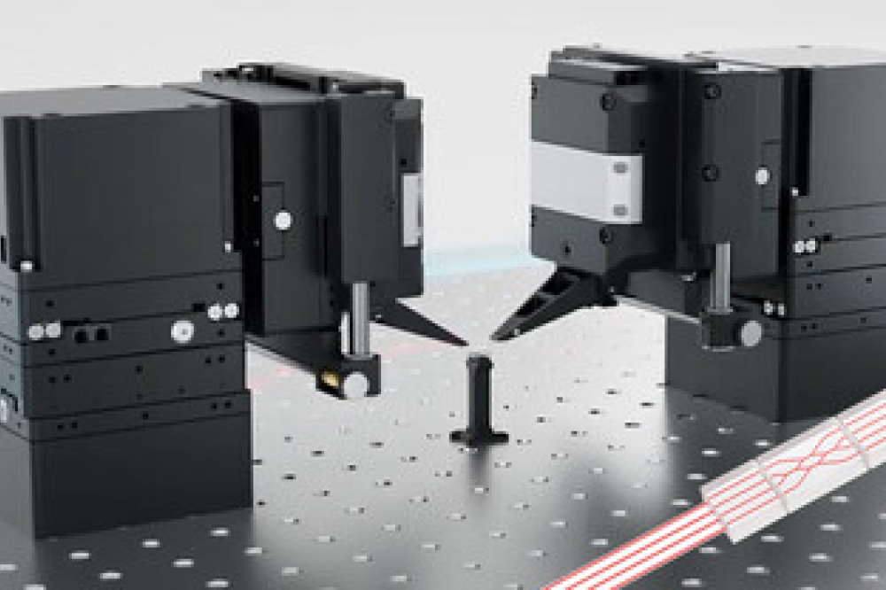
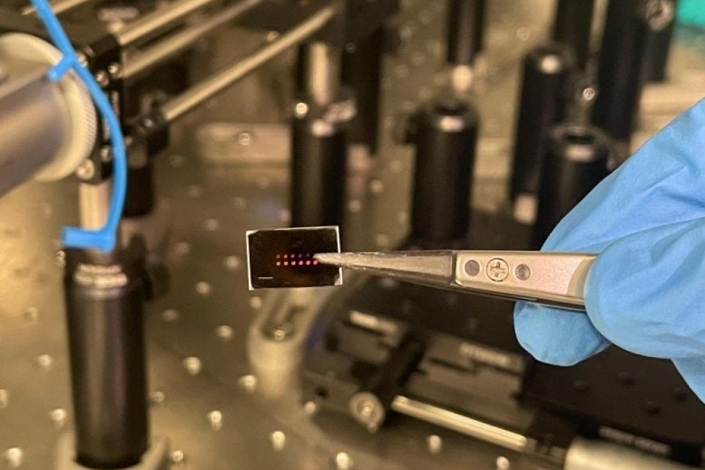
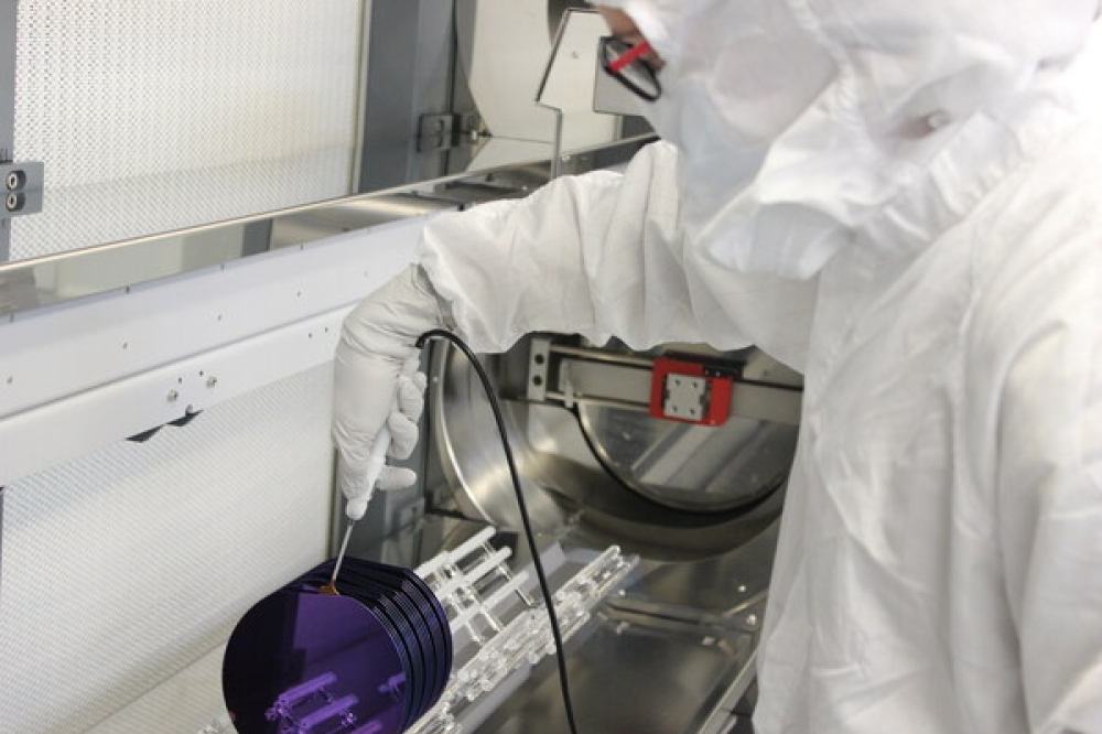
Figure 2. Wafer-level PIC testing at VLC Photonics.
Research and Development:
Spain has several research and development centers working in the field of photonics and optical engineering. These include CD6 - Centre for Sensors, Instruments and Systems Development, a spin-off from the University Polytechnic of Catalunya which focuses on the areas of metrology, visual optics, optical design & simulation, and colour; and also FYLA, based in Valencia and Barcelona who make lasers and systems for a multitude of applications from hyperspectral imaging and metrology to optical communication and material processing. The two most important research organizations in photonics are the Institute of Optics in Madrid, part of the Spanish government’s network of research centers, and the world-renown ICFO - The Institute of Photonic Sciences founded in 2002 in Catalunya.
Frontend Integration:
The Institute of Microelectronics of Barcelona (IMB-CNM) has developed a silicon nitride (SiN) Photonic Platform for PIC prototyping. Their mission is to carry out applied research based on micro and nanotechnologies, mainly focused on the development of components and micro and nano systems. The infrastructure and equipment allow for the development of processes for the realization and characterization of photonic and electronic: micro-nano devices, integrated circuits, and micro-nano systems intended for research, development, and technology transfer to industry.
Backend Integration:
UPVfab, located at the University Polytechnic of Valencia has a micro-fabrication R+D and pilot line cleanroom facility. Their mission is to perform transversal activities to serve and educate the academic and industry communities about micro- and nano-fabrication. UPVfab together with the IMB-CNM has developed a versatile, moderate confinement Silicon Nitride platform for photonic integrated applications, running under a Multi-Project Wafer scheme or dedicated runs. The facility comprises 500 m2 cleanrooms ISO-7 (class 10.000) and positions with automation tools for the backend processing of semiconductor wafers.
Chip Design and Testing:
VLC Photonics is a world-leading engineering company offering a full range of services for the development of Photonic Integrated Circuits (PICs), with a focus on design in testing at both die and wafer levels. The current service portfolio includes techno-economic feasibility studies and consultancy, in-house PIC design, characterization and test, and full PIC prototyping through external manufacturing and packaging/assembly partners. VLC Photonics, as a pure-play fabless design house, works with multiple foundries and has expertise in all the main photonic integration technologies, including Silicon-on-insulator, PLC, SiN, InP, LNOI, and GaAs. VLC Photonics also works closely with foundries in the development of their Process Design Kits (PDKs), allowing external users to easily access their manufacturing capabilities. The organization has world-leading capabilities for RF testing up to 110 GHz and has also provided unique edge-coupling wafer-level testing since 2020. VLC Photonics is part of Hitachi, Ltd.
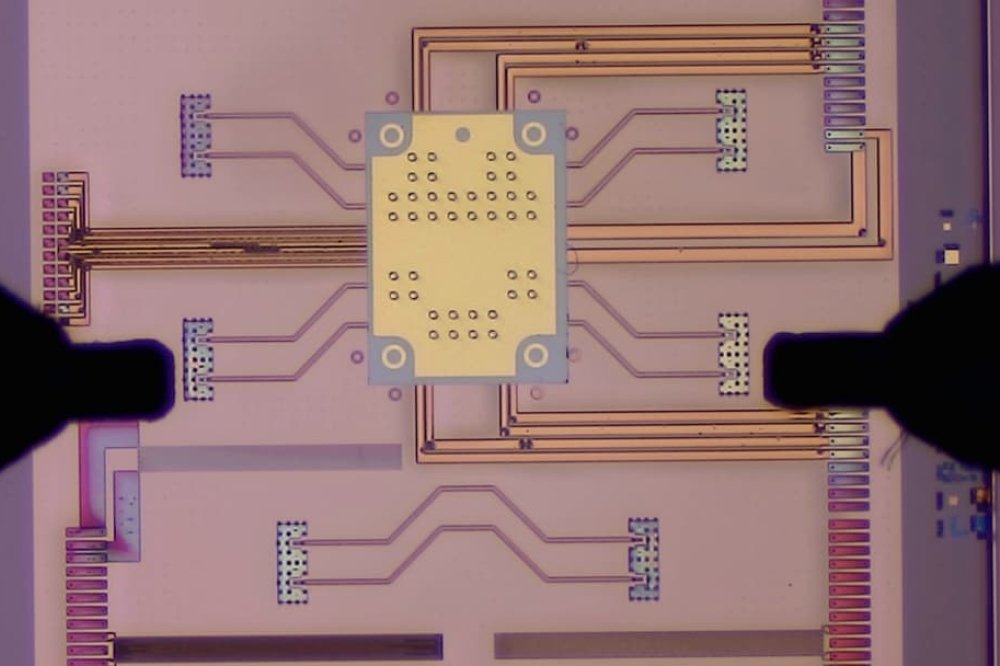
Figure 3. Photonic layout of the iPronics´ SPPGA-based SmartLight Processor.
Field Programmable Photonic Gate Arrays:
iPronics, a spinoff company from the University Polytechnic of Valencia, Spain is developing the innovative concept of Field Programmable Photonic Gate Arrays (FPPGAs), which are based on common optical hardware configurable through software to perform multiple functions. iPronics is working on the development of future information processing systems where electronics and photonics work cooperatively by synergistically exploiting the best capabilities of each technology. Applications include 5G and 6G telecommunications, data center interconnection, artificial intelligence, signal processing, sensing, and quantum information.
III-V semiconductors foundry:
The city of Vigo in Spain will be the location of a new state-of-the-art foundry for III-V-Semiconductor-based photonics called SPARC. This new company will consist of a 1.600 m2 cleanroom for wafer production and a research center that will assist customers in bringing fully-certified photonic products to the market. The foundry expects to be operational around late 2023 and SPARC aims to capitalize on the potential of III-V to accommodate the increasing number of markets and applications that rely heavily on light, photonics, and high-speed electronics. III-V Semiconductors are the only class of materials that can be used to realize very compact- and efficient light sources and detectors across a very wide wavelength range from the ultraviolet up to the mid-infrared.
Consequently, SPARC will have the capability and capacity to address a large customer base across a wide range of different markets, including optical communications, displays, lighting, aerospace, automotive, biomedical, sensing, and quantum technologies, as well as high-speed- and/or high-power electronic applications for which the III-V Semiconductor technology is equally well suited for. From this brief overview, it can be seen that while missing the capabilities in traditional chip manufacturing Spain has a well-established organic ecosystem in the production of photonic chips. With the right level of investment, and if the right decisions are taken – this country famous for its beautiful weather and cheerful people could also become the European reference in photonic integration.
Further reading
[1] https://www.eetimes.eu/spain-approves-e12-25b-semiconductor-investment-plan/
[2] https://www.bloomberg.com/news/articles/2022-08-02/spain-short-on-takers-for-12-billion-in-semiconductor-subsidies
[3] https://www.euronews.com/next/2022/03/15/intel-set-to-build-a-new-17-billion-chip-manufacturing-hub-in-germany-as-it-pours-money-in


