

Yield improvement techniques in the manufacturing of AWG (Cascade) PLC
The AWG Cascade chip offers a step improvement over the conventional
AWG. In this article Broadex Technologies discusses how the AWG Cascade
chip works, where it will be deployed and how it can be manufactured
with a good yield.
BY HENK BULTHUIS, BROADEX TECHNOLOGIES UK
AWG Cascade products consist of two synchronized Silica-on-Silicon Array Waveguided Gratings (AWGs), arranged in series on a single chip. Arrayed Waveguide Gratings are working as a prism that disperse the light coming into the device when coupled to an input fiber. For AWG Cascade (CAWG) chips the dispersion of the two AWGs are synchronized which gives a theoretical zero loss over a wide passband. The small footprint allows the chip to be integrated in small form factor transceivers which make up the workforce of datacenters for data transport, internal between the racks, from rack to rack and even from datacenter to datacenter.

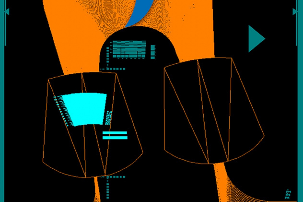
AWG Cascade or CAWG chip in transceiver package
In the illustration below, light enters the chip from a fiber to the input waveguide on the left-hand side. The four receiver channels on the right side of the chip connect to high-speed photodetectors and each photodetector captures a different slice of the optical spectrum. This way the chip is used to demultiplex the 4 channels from the input fiber, each channel carrying its own portion of data. The slicing action of the spectrum for each of the 4 receive channels is displayed in the transmission spectrum.

Layout of an approximately 10 mm long AWG cascade chip for CWDM4 transceiver.
The fiber can now carry 4 times more information compared to using only a single frequency of light. AWGs and CAWGS can be designed to Multiplex and or Demultiplex anywhere between 4 and 96 channels, thus multiplying the capacity of a fiber connection by a factor 4x to 96x respectively without need to grow the fiber plant. Compared to regular AWG, the AWG Cascade produces ultra-low insertion loss, flat-top bandpass shape while maintaining a single mode output. The single mode output allows for efficient coupling to ever increasing high-speed photodetectors which have ever decreasing active area sizes as the speed of switches, or baud rate, increases. Suitable for WDM applications, they can be used as both a MUX, to combine say the light of 4 lasers on a single fiber, or DEMUX, to separate the light from a single fiber to 4 individual detectors.

Figure above: Simulated transmission spectrum of Cascade AWG.
The curved AWG Cascade structure can also be laid out very efficiently to provide up to 16 individual AWG Cascade structures on a single chip, see figure, which is of a similar size (10x20mm) as a typical fiber block array that is conventionally used to couple light from chip to fiber. This dense footprint and the flexibility to adjust the mode field diameter, minimizing coupling loss, is ideal for Co-Packaged Optics (CPO) used in next generation multi-Terabit applications.
Yield improvement for AWG Cascade manufacturing: Even though semiconductor processes are used for manufacturing of PLC (Planar Lightwave Circuits) the yield is not just limited by defects. The wave-type nature of the photons that travel the channels on the chip means that the function of the chip is very sensitive to the exact pathlength that photons travel. When the photons are separated and combined they need to arrive exactly in phase. If the light path traveled by photons in one channel is off by a femtosecond this will already cause destructive interference of the photons causing the chip to fail specification.
During etching of the waveguides the width of the waveguides may vary due to local varying etch chemistry. Other nonuniformities may arise from imaging errors due to photo, wafer bow, resist spin, refractive index and thickness variation during deposition of the layers.

An array of 16 individual AWG Cascade structures for next generation multi-Terabit applications using Co-Packaged Optics (CPO).
All these variations impact the transit time, or phase, of the photons on the chip. These phase errors are equivalent to imaging errors which are the main cause of failing chips. Defects cause amplitude errors which are sporadic compared to phase errors. In the figure we show a typical sickle-shaped phase error across the branches that make up the array section of an AWG.
Very similar to the imaging errors when fabricating discrete lenses, you can have parabolic phase errors that cause a defocus or blurring of the image. One can also have third order phase errors, or COMA, that cause a ghost image slightly displaced relative to the main image. In practice, in order to make a yielding chip one should eliminate at least the first, second and third order imaging errors. At Broadex Technologies we have developed an industrial approach to testing and eliminating these phase errors in order to improve the yield.
We use a tuneable laser scan to the transfer function of the chip at test. Fourier transform of the transfer function gives time response. The time response gives delay errors which are the equivalent of the phase errors causing the aberrations in the function of the AWG. Correction and monitor of phase errors are subsequently automated for our AWG chips in order to get good yield for volume products.
The UV Trimming system is based around a high power UV laser and PC controlled stages. Before trimming the chips are saturated with hydrogen. During the trim, the laser causes the hydrogen to react within the Germanium doped waveguiding glass, modifying the refractive index of the material by about 4e-3, which is enough to allow for the order of femtosecond delay corrections by writing arbitrary shapes of the order of 100um using a programmable stage.
The alignment and setup is manual while trim design and implementation is automated. It is also possible to make the phase corrections for each of the two orthogonal polarization states of light. In the future these corrections can be made using wafer level testing and wafer level trimming.

A typical sickle-shaped phase error across the branches of the AWG
Due to routine testing of all chips that run in the operations we frequently find that depending on the location on the wafer, and depending on the design, systematic phase errors are created that are signature of the specific combination of channel density and processing equipment.
These systematic phase errors are not eliminated by UV trimming but by design. Even though we can make every chip work by UV trimming, provided there are no defects on the channels where the photons travel, it is still economical to eliminate the systematic phase errors beforehand. Using the data from the phase measurements, routine adjustments in the design are made during the exposure of the photoresist for each individual chip depending on location. It is shown here how we correct for a systematic phase error on one particular device.

Correction of the phase error
In the fabrication of AWG Cascade chip it is important that the dispersion of the first and second AWG of the Cascade are perfectly synchronized. If that is not the case the transmission passband will suffer high insertion loss. Again using the
UV trimming procedure outlined in this article we can repair the passband by UV trimming. Such a correction, and how the passband recovers is illustrated in the following figure.

Correction of the phase error

Figure: left the distribution of phase versus channel number before, and right after correction.

Figure: CAWG response before (left) and after (right) aligning the two AWGs in the Cascade.
Conclusion
We have discussed the manufacturing of AWG Cascade chips for Multiplexing and Demultiplexing function. It is demonstrated that the chip possesses a passband that is wide, has low loss and works for single mode transmission.
Distributions in performance of these chips, and other types of AWG chips, are observed from the process variation inherent in the manufacturing methods used in the chip manufacturing process. Such variation, whether within wafer or wafer to wafer can be addressed through modification of the manufacturing process to remove systematic phase errors, or by laser trimming the chips to eliminate the remaining phase errors in the chips one by one. The testing and trimming of phase errors has been automated in order to essentially allow all defect-free chips to pass specification.
Figure, CAWG response before (left) and after (right) aligning the two AWGs in the Cascade.


